Nonvolatile semiconductor memory device and write-in method thereof

a nonvolatile semiconductor and memory device technology, applied in static storage, digital storage, instruments, etc., can solve the problems of shortened programming time, varying programming speed, and widening the threshold voltage distribution, so as to achieve the effect of high-speed rewriting characteristic and reduced threshold voltage distribution

Active Publication Date: 2013-07-11
POWERCHIP SEMICON MFG CORP
View PDF4 Cites 17 Cited by
  • Summary
  • Abstract
  • Description
  • Claims
  • Application Information

AI Technical Summary

Benefits of technology

[0039]Therefore, according to a non-volatile semiconductor memory device and a write-in method thereof of the invention, a programming speed is detected during writing-in to the memory cell array before or after an erasing process where data of written-in memory cells is erased. Also, a programming start voltage is determined corresponding to the programming speed for every block or every word line. The determined programming start voltage is stored in the memory cell array and the programming start voltage is read-out from the memory cell array to write-in predetermined data. Accordingly, variation of the threshold voltage distribution after programming is minimized and a high-speed rewriting characteristic can be obtained.
[0040]A detailed description is given in the following embodiments with reference to the accompanying drawings.

Problems solved by technology

In addition, if a higher programming start voltage Vstart is used, the programming time is shortened, and there would be a problem that the threshold voltage distribution would become wider.
Moreover, after cycles of programming and erasing, if the programming start voltage Vstart is the same, the threshold voltage distribution becomes wider, and there would be a problem that a programming speed would varies depending of word lines in blocks of a memory cell array.
Therefore, optimization of the programming start voltage Vstart is an important issue.
Accordingly, durability gets worse because of the degradation of the oxide film along with data rewriting, resulting in a problem where it is difficult to obtain a high-speed multi-rewriting characteristic.
Regarding FIG. 11, as it is clearly shown from FIG. 6, when the same programming start voltage Vstart is used in every block for programming, there's a problem that the threshold voltage distribution varies.

Method used


Image

  • Nonvolatile semiconductor memory device and write-in method thereof
  • Nonvolatile semiconductor memory device and write-in method thereof
  • Nonvolatile semiconductor memory device and write-in method thereof

Examples


first embodiment

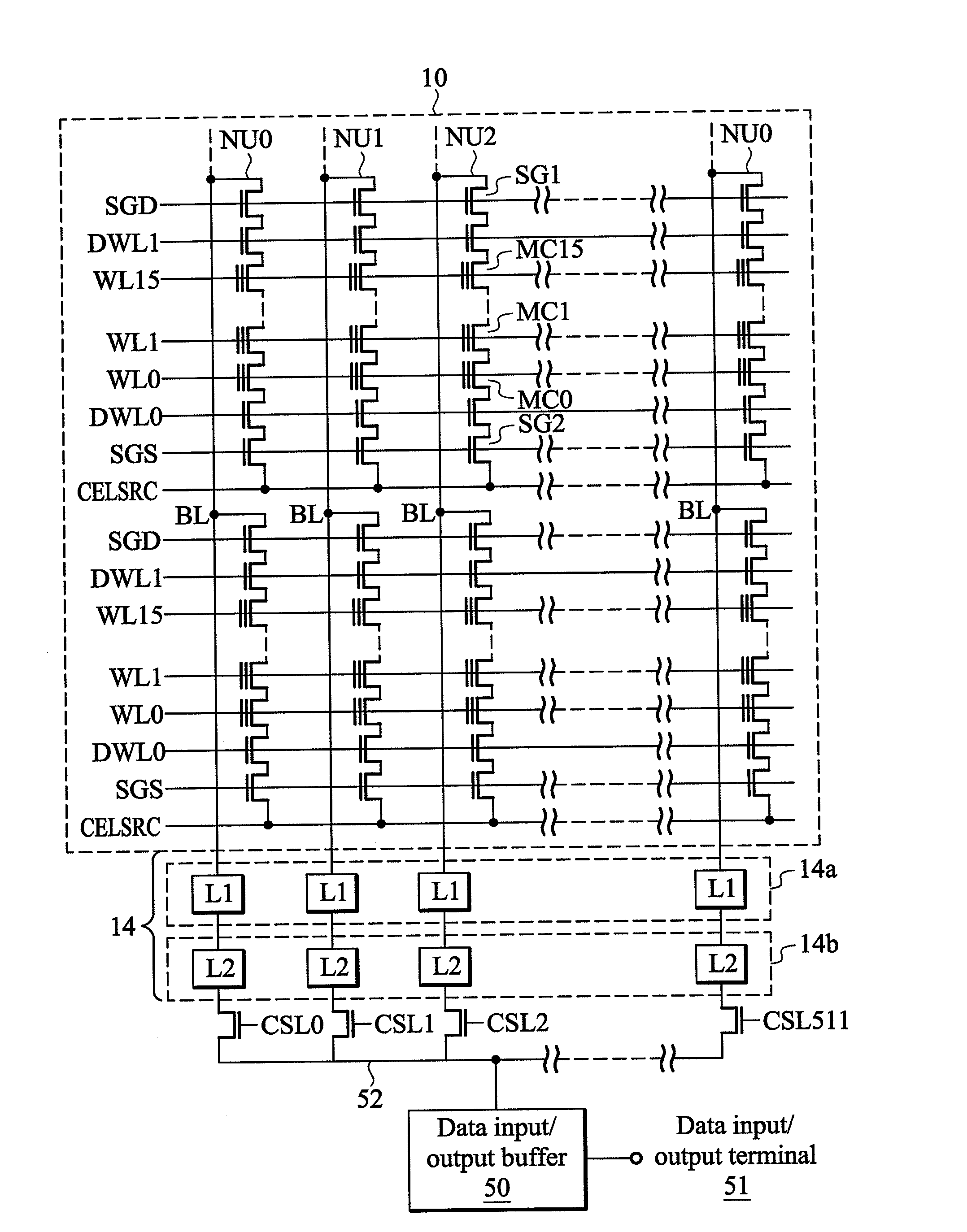
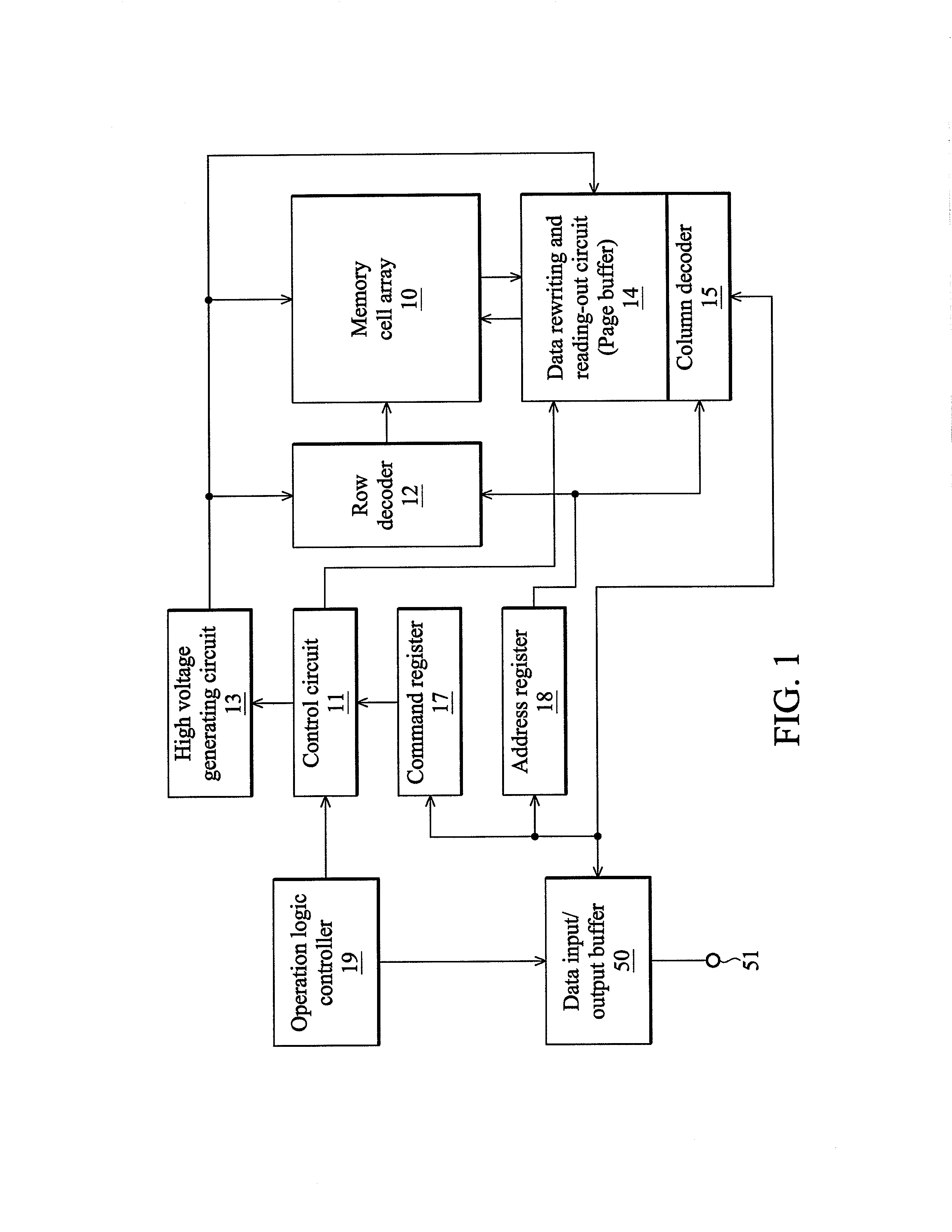
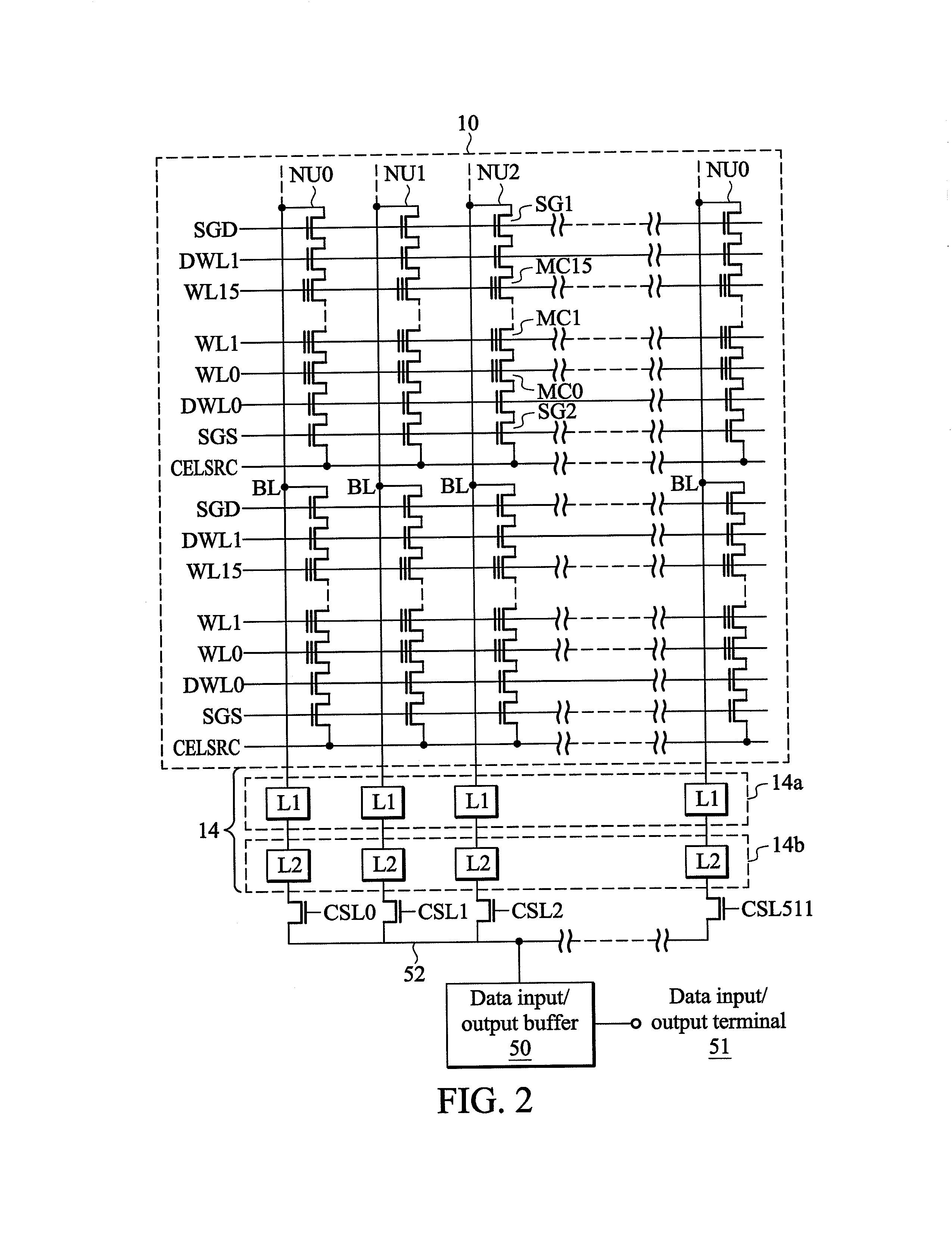
[0084]FIG. 13 is a flowchart showing a programming process according to the invention. In FIG. 13, first, programming data is loaded in step S1. In step S2, data of specific bits of a block selected for write-in is read out before a programming pulse is applied. Vstart of the block or each word line of the block is stored in the data. More specifically, first, as mentioned above, when the data is stored in a dummy word line, the dummy word line is selected and read-out. When the data is stored in normal word lines where additional memory cells are added, after a predetermined reading-out voltage Vsp is applied to all word lines, reading-out is performed once. Then, a programming start voltage and flag data are set to a temporary register (buffer memory) based on data of specific bits corresponding to selected word lines. Next, in step S3, the programming data is set to the buffer memory 14a. Furthermore, in step S4, a programming process using an ISPP method using the programming st...

second embodiment

[0092]FIG. 19 is a flowchart showing an erasing process according to the invention. In FIG. 19, first, an old programming start voltage and flag data are read out from specific bits of memory cells in step S61. Here, a flag denotes a word line for a programming speed checking. Next, the programming speed checking process is performed in step S62. Data is erased by using an erasing pulse in step S63. Then, in step S64, a soft programming process is performed by using a soft programming start voltage based on the programming start voltage set by said programming speed checking or a soft programming start voltage determined by other predetermined ways. Further, in step S65, the programming start voltage and the flag data set as described above are stored in specific bits, and the modified flag denotes a next checking word line for the programming speed checking.

[0093]In the programming speed checking process of FIG. 19, in order to reduce extra time for the programming speed checking p...


PUM


Abstract

TASK: to minimize variations of the threshold voltage distribution after programming and obtain a high-speed rewriting characteristic. MEANS FOR SOLVING THE PROBLEM: A non-volatile semiconductor memory device includes a non-volatile memory cell array and a control circuit for controlling writing-in to the memory cell array, wherein before or after an erasing process where data of written-in memory cells is erased, the control circuit detects a programming speed when writing-in to the memory cell array, determines a programming start voltage corresponding to the programming speed for every block or every word line, stores the determined programming start voltage in the memory cell array and reads-out the programming start voltage from the memory cell array to write-in predetermined data.

Description

CROSS REFERENCE TO RELATED APPLICATIONS[0001]This Application claims priority of Japan Patent Application No. 2012-001495, filed on Jan. 6, 2012, the entirety of which is incorporated by reference herein.BACKGROUND OF THE INVENTION[0002]1. Field of the Invention[0003]The invention relates to an electrically rewritable non-volatile semiconductor memory device (EEPROM), such as a flash memory, etc, and a write-in method thereof.[0004]2. Description of the Related Art[0005]A highly integrated NAND-type non-volatile semiconductor memory device (refer to Patent Documents 1-4) which connects a plurality of memory cell transistors (hereinafter referred to as memory cells) to and between bit lines and source lines in series to form a NAND string is well known in the art.[0006]In a common NAND-type non-volatile semiconductor memory device, when erasing, a high voltage, such as 20V, is applied to a semiconductor substrate and 0V is applied to a word line. As such, electrons are pulled out fro...

Claims


Application Information

Patent Timeline
Patent Type & Authority Applications(United States)
IPC IPC(8): G11C16/10
CPCG11C16/20G11C16/10
Inventor SENOO, MAKOTOARAKAWA, HIDEKISHIROTA, RIICHIRO
Owner POWERCHIP SEMICON MFG CORP
Why Eureka
Try Eureka