Electronic component and method for manufacturing the same
a technology of electronic components and manufacturing methods, applied in the direction of printed circuit aspects, semiconductor/solid-state device details, cross-talk/noise/interference reduction, etc., can solve the problems of increasing manufacturing costs and imposing constraints on substrate design, and achieve the effect of facilitating more flexibility in substrate design and reducing manufacturing costs
- Summary
- Abstract
- Description
- Claims
- Application Information
AI Technical Summary
Benefits of technology
Problems solved by technology
Method used
Image
Examples
example 1
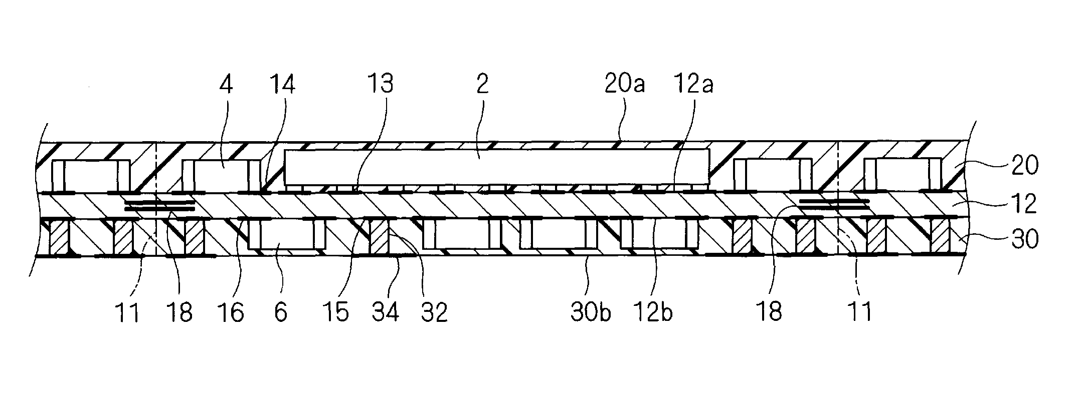
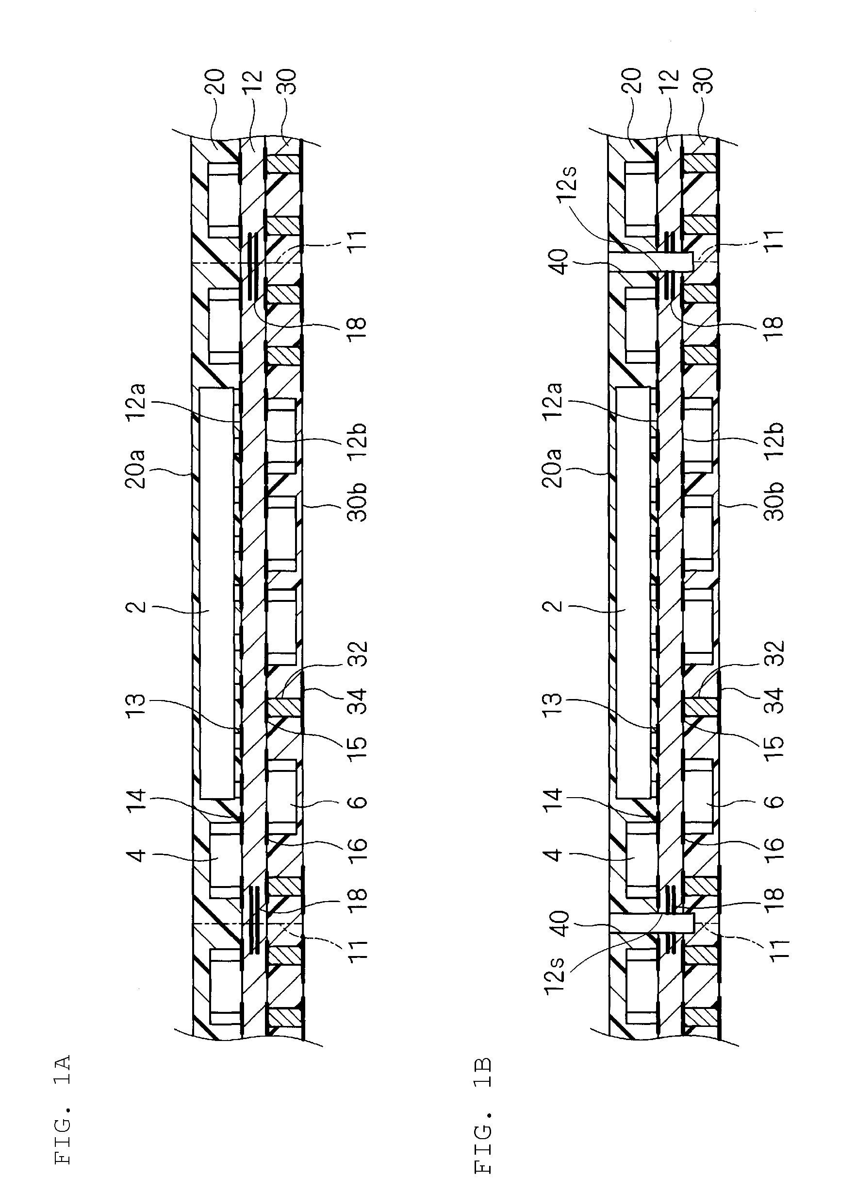
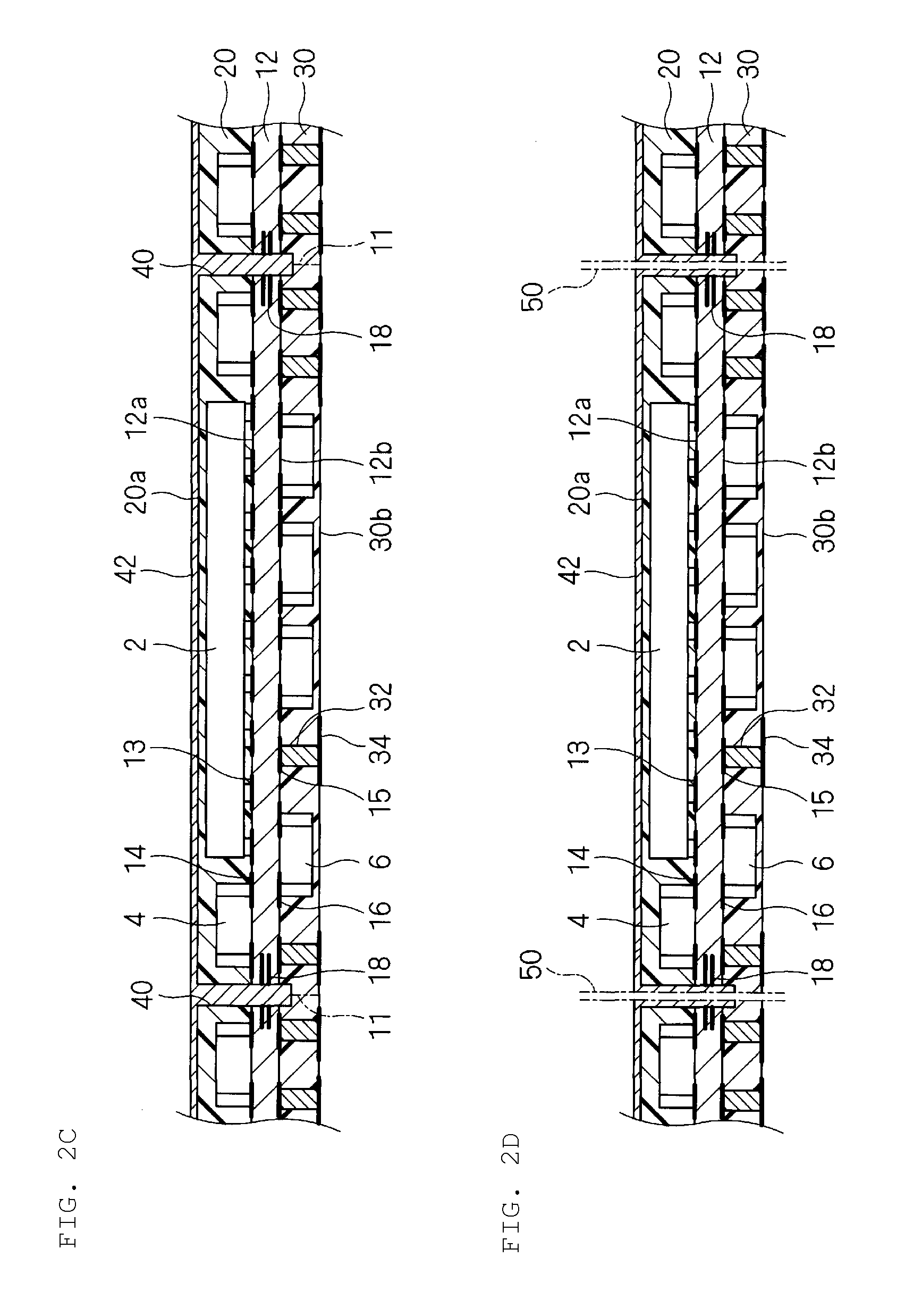
[0025]An electronic component 10 of Example 1 of a preferred embodiment of the present invention will now be described with reference to FIG. 1A-FIG. 4.
[0026]FIG. 4 is a cross-sectional diagram of the electronic component 10. As illustrated in FIG. 4, in the electronic component 10, a top surface 12a that serves as a first principle surface of a substrate 12 and first electronic components 2, 4 mounted on the top surface 12a are coated with a first resin layer 20. Furthermore, a bottom surface 12b that serves as a second principle surface of the substrate 12 and second electronic components 6 mounted on the bottom surface 12b are coated with a second resin layer 30. The electronic components 2, 4, 6 to be mounted on the top surface 12a and the bottom surface 12b of the substrate 12 are surface mount components, and may be, for example, active devices such as semiconductors, etc., or passive devices such as capacitors, inductors, resistors, etc. The electronic components 2, 4, 6 are ...
example 2
[0063]An electronic component 10a of Example 2 will now be described with reference to FIG. 5. FIG. 5 is a cross-sectional diagram of the electronic component 10a.
[0064]As illustrated in FIG. 5, the electronic component 10a of Example 2 preferably is formed in substantially the same manner as the electronic component 10 of Example 1. Below, the same reference numerals denote the same elements as those of Example 1, and the description will focus on differences from Example 1.
[0065]The electronic component 10a of Example 2 is, when compared to the electronic component 10 of Example 1, formed such that the entirety of a side surface 30t of the second resin layer 30 forms a single plane together with the side surface 12s of the substrate 12 and the side surface 20s of the first resin layer 20, and such that a surface level difference 44t is formed between a side surface 44s of a shield layer 44 and the side surface 30t of the second resin layer 30.
[0066]The electronic component 10a ma...
example 3
[0069]An electronic component 10b of Example 3 will now be described with reference to FIG. 6. FIG. 6 is a cross-sectional diagram of the electronic component 10b.
[0070]The electronic component 10b of Example 3 may be manufactured by using substantially the same steps as those of the electronic component 10 of Example 1. That is, the electronic component 10b preferably is manufactured by using the same steps as those of Example 1 except that a shield layer 46 is formed by sputtering in the third step of manufacturing the electronic component 10 of Example 1.
[0071]The shield layer 46 is a metal film, and thus formed to thinly cover surfaces of inner walls and the bottom of the closed-bottom trench 40. As a result, in the shield layer 46, a step surface 46t is formed along the bottom of the closed-bottom trench 40. The step surface 46t is continuous with a side surface 46s that is formed along the surface of the inner wall of the closed-bottom trench 40.
[0072]In the electronic compon...
PUM
| Property | Measurement | Unit |
|---|---|---|
| electrically conductive | aaaaa | aaaaa |
| structure | aaaaa | aaaaa |
| electrically | aaaaa | aaaaa |
Abstract
Description
Claims
Application Information
 - R&D
- Intellectual Property
- Life Sciences
- Materials
- Tech Scout
- Unparalleled Data Quality
- Higher Quality Content
- 60% Fewer Hallucinations
Browse by: Latest US Patents, China's latest patents, Technical Efficacy Thesaurus, Application Domain, Technology Topic, Popular Technical Reports.
© 2025 PatSnap. All rights reserved.Legal|Privacy policy|Modern Slavery Act Transparency Statement|Sitemap|About US| Contact US: help@patsnap.com


