
DC offset cancelation circuit

a cancellation circuit and offset technology, applied in the direction of dc-coupled stages of dc-amplifiers, low noise amplifiers, pulse automatic control, etc., can solve the problems of difficult implementation of integrated circuits, severe dc offset, and degraded isolation characteristics, so as to facilitate the selection of pass frequencies

Inactive Publication Date: 2013-05-16
SAMSUNG ELECTRO MECHANICS CO LTD
View PDF11 Cites 1 Cited by
  • Summary
  • Abstract
  • Description
  • Claims
  • Application Information

AI Technical Summary

Benefits of technology

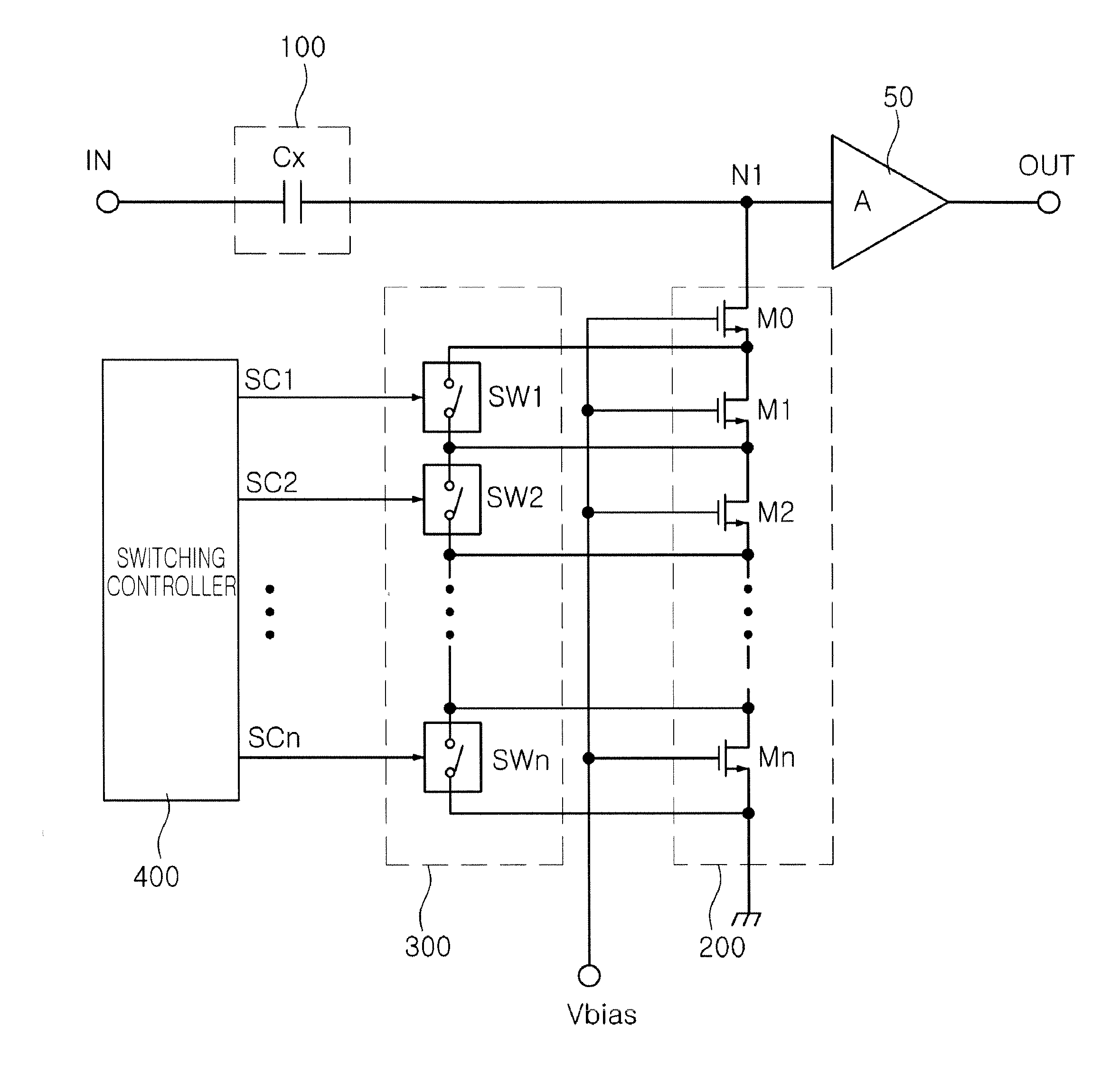
The present invention provides a circuit that cancels out DC offset in a direct conversion receiver system. It can be implemented as an integrated circuit using a resistor in a linear region, and it can easily select a pass frequency.

Problems solved by technology

In particular, in a case in which a low noise amplifier (LNA) / mixer is simultaneously fabricated with an oscillator such as in a DVB-S system, or the like, isolation characteristics are degraded, and the DC offset becomes severe due to phenomena such as substrate coupling, ground bounce, bond wire radiation, capacitive and magnetic coupling, and the like.
Here, a cut-off frequency Fc is defined as ‘1 / (2πRC)’, and in order to cancel a low frequency DC component, a capacitor having a high capacitance value should be used, making it difficult to implement an integrated circuit.
Also, even when a feedback circuit is implemented as an analog circuit without the A / D converter or the D / A converter, a complicated analog circuit is implemented, increasing the area of the circuit as much.
Also, in terms of the characteristics of the feedback structure, current consumption and a chip size are increased.
As described above, when the DC offset cancellation structure using a high pass filter is employed in the direct conversion system, the values of a capacitor and a resistor that decide (or control) the cut-off frequency of the high pass filter must be great to obtain frequency characteristics close to a DC, but it is difficult to increase the size of the resistor or the capacitor unlimitedly due to the limited chip size.

Method used


Image

  • DC offset cancelation circuit
  • DC offset cancelation circuit
  • DC offset cancelation circuit

Examples


Embodiment Construction

[0035]Embodiments of the present invention will now be described in detail with reference to the accompanying drawings. The invention may, however, be embodied in many different forms and should not be construed as being limited to the embodiments set forth herein. Rather, these embodiments are provided so that this disclosure will be thorough and complete, and will fully convey the scope of the invention to those skilled in the art. In the drawings, the shapes and dimensions of elements may be exaggerated for clarity, and the same reference numerals will be used throughout to designate the same or like components.

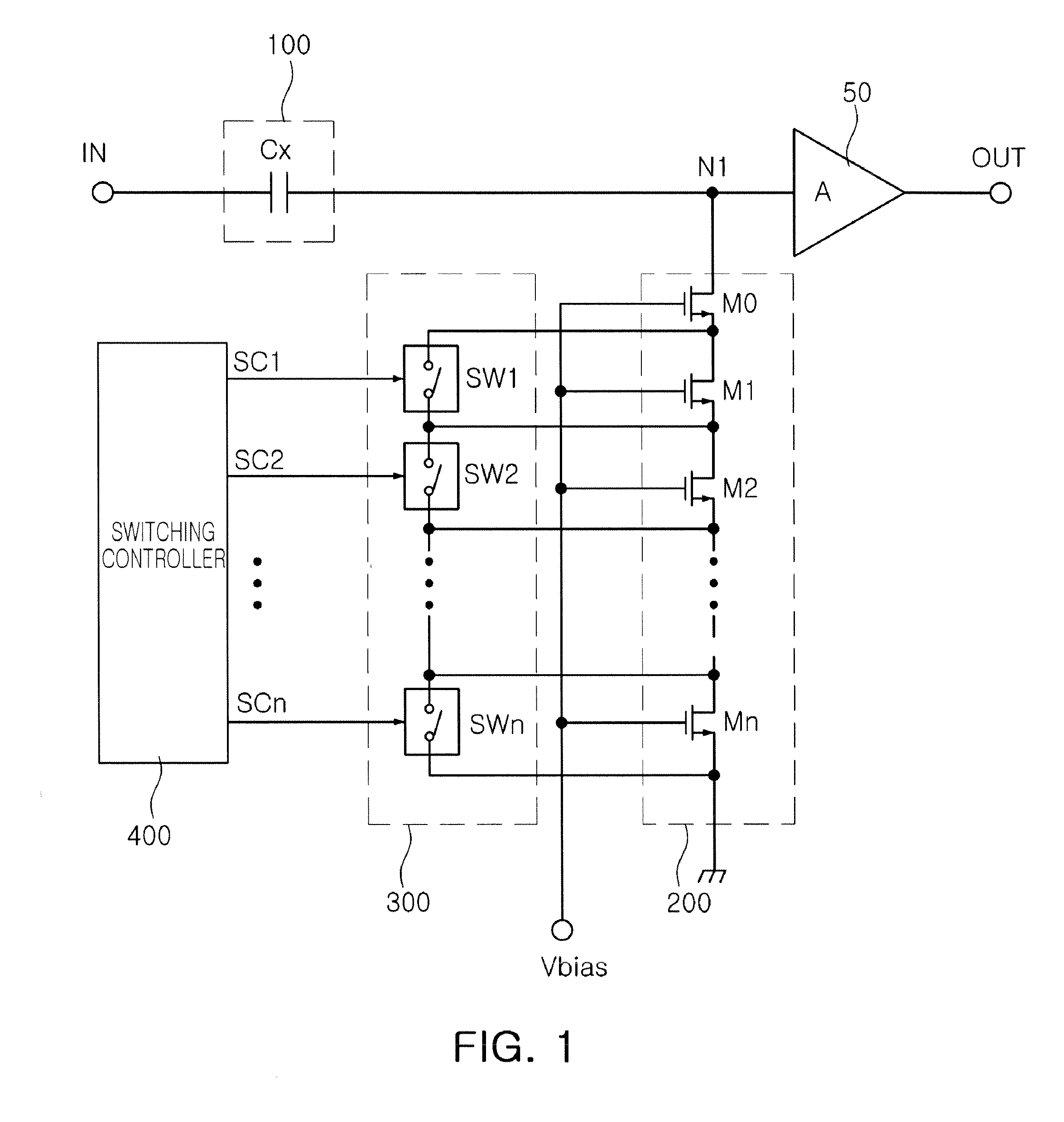
[0036]FIG. 1 is a schematic block diagram of a DC offset cancellation circuit according to an embodiment of the present invention.

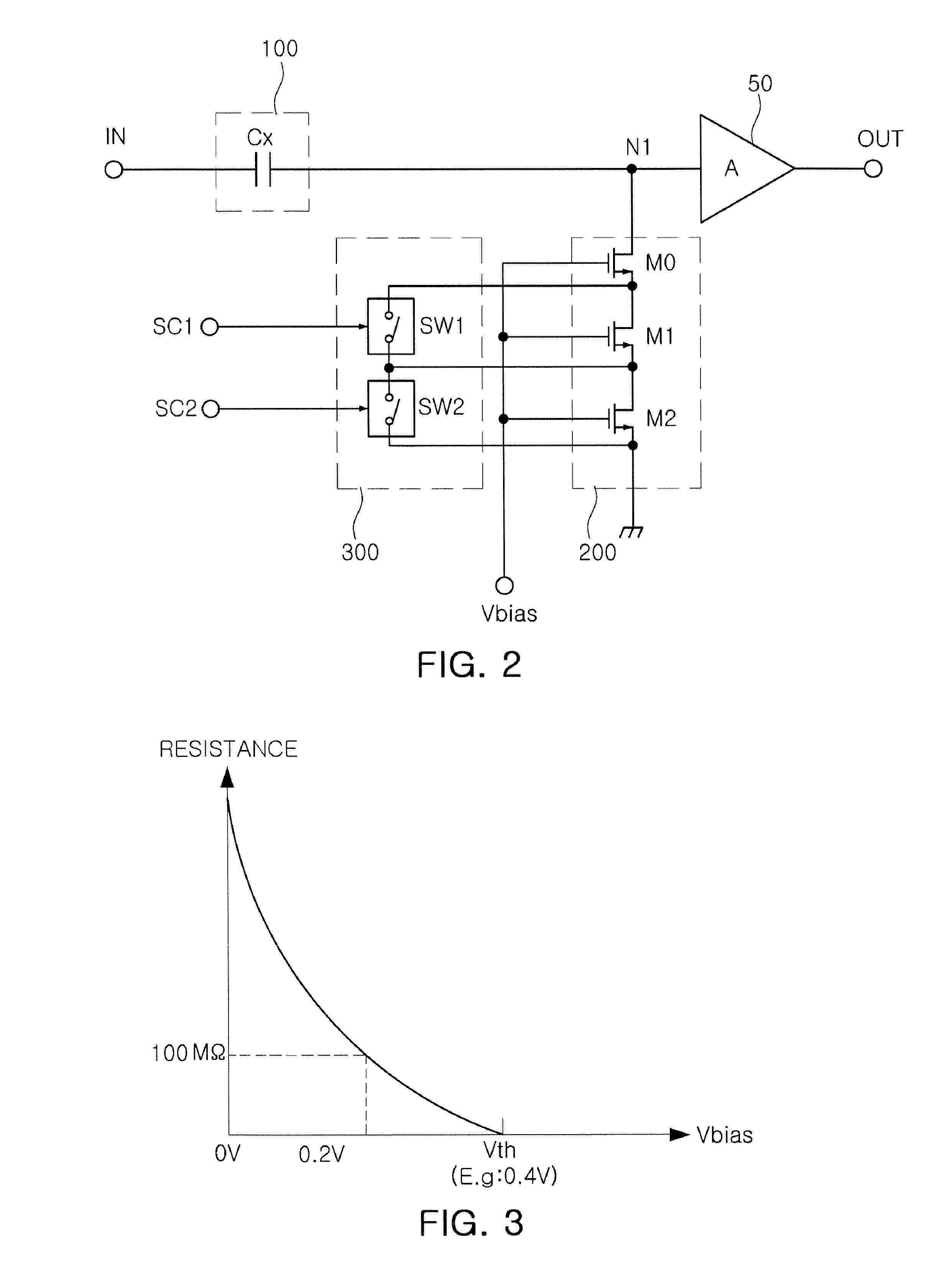
[0037]With reference to FIG. 1, a DC offset cancellation circuit according to an embodiment of the present invention may include: a capacitor circuit unit 100 including at least one capacitor connected between an input terminal IN and an amplifi...


PUM


Abstract

There is provided a DC offset cancellation circuit including: a capacitor circuit unit including at least one capacitor connected between an input terminal and an input of an amplifier; a MOSFET circuit unit including a plurality of MOSFETs connected in series between a first connection node connected to a predetermined one of both terminals of the capacitor circuit unit and a ground and operating in a linear region; and a switching circuit unit including a plurality of switch elements for selecting several MOSFETs previously selected from among the plurality of MOSFETs of the MOSFET circuit unit, respectively.

Description

CROSS-REFERENCE TO RELATED APPLICATIONS[0001]This application claims the priority of Korean Patent Application No. 10-2011-0117401 filed on Nov. 11, 2011, in the Korean Intellectual Property Office, the disclosure of which is incorporated herein by reference.BACKGROUND OF THE INVENTION[0002]1. Field of the Invention[0003]The present invention relates to a DC offset cancellation circuit applicable to a direct conversion receiver (DCR) system and which can be implemented as an integrated circuit (IC) by using a resistor in a linear region of a MOSFET, and can easily select a pass frequency.[0004]2. Description of the Related Art[0005]In general, a DC offset in a direct conversion structure of a communications system may negatively affect signals and should be solved. A DC offset is generated in the process of converting an RF signal into a baseband signal, acting as in-band interference.[0006]In particular, in a case in which a low noise amplifier (LNA) / mixer is simultaneously fabrica...

Claims


Application Information

Patent Timeline
Patent Type & Authority Applications(United States)
IPC IPC(8): H03L5/00
CPCH03F3/189H03F2200/252H03F2200/294H03F2200/42H03H7/0153H03F3/34H04B1/10
Inventor NA, YOO SAMYOO, HYUN HWAN
Owner SAMSUNG ELECTRO MECHANICS CO LTD
Learn More