
Method for adjusting voltage characteristics of semiconductor memory element, method for adjusting voltage characteristics of semiconductor memory device, charge pump and method for adjusting voltage of charge pump

a technology of semiconductor memory and voltage characteristics, which is applied in the direction of digital storage, process and machine control, instruments, etc., can solve the problems of adding complexity to the manufacturing process, and achieve the effects of increasing the threshold voltage, improving the voltage characteristics of the semiconductor memory device, and increasing the threshold voltag

Inactive Publication Date: 2013-05-09
SEMICON TECH ACADEMIC RES CENT
View PDF0 Cites 5 Cited by
  • Summary
  • Abstract
  • Description
  • Claims
  • Application Information

AI Technical Summary

Benefits of technology

The present invention provides methods for adjusting the voltage characteristics of a semiconductor memory device in a simple way to improve its operating characteristics. The method includes steps of performing a write operation, a low voltage read operation, adjusting voltage levels to increase the threshold voltage of certain memory elements, and performing an after-third-step write operation. This method can make the voltage characteristics of the semiconductor memory device more efficient and effective. The charge pump and method of adjusting its voltage can also improve the operation of the semiconductor memory device.

Problems solved by technology

However, since the voltage characteristics adjusting method described above requires formation of the halo regions, application of the voltage characteristics adjusting method to an SRAM or a charge pump requires additional processes such as an impurity doping process in manufacturing, which adds the complexity to the manufacturing process.

Method used


Image

  • Method for adjusting voltage characteristics of semiconductor memory element, method for adjusting voltage characteristics of semiconductor memory device, charge pump and method for adjusting voltage of charge pump
  • Method for adjusting voltage characteristics of semiconductor memory element, method for adjusting voltage characteristics of semiconductor memory device, charge pump and method for adjusting voltage of charge pump
  • Method for adjusting voltage characteristics of semiconductor memory element, method for adjusting voltage characteristics of semiconductor memory device, charge pump and method for adjusting voltage of charge pump

Examples


first embodiment

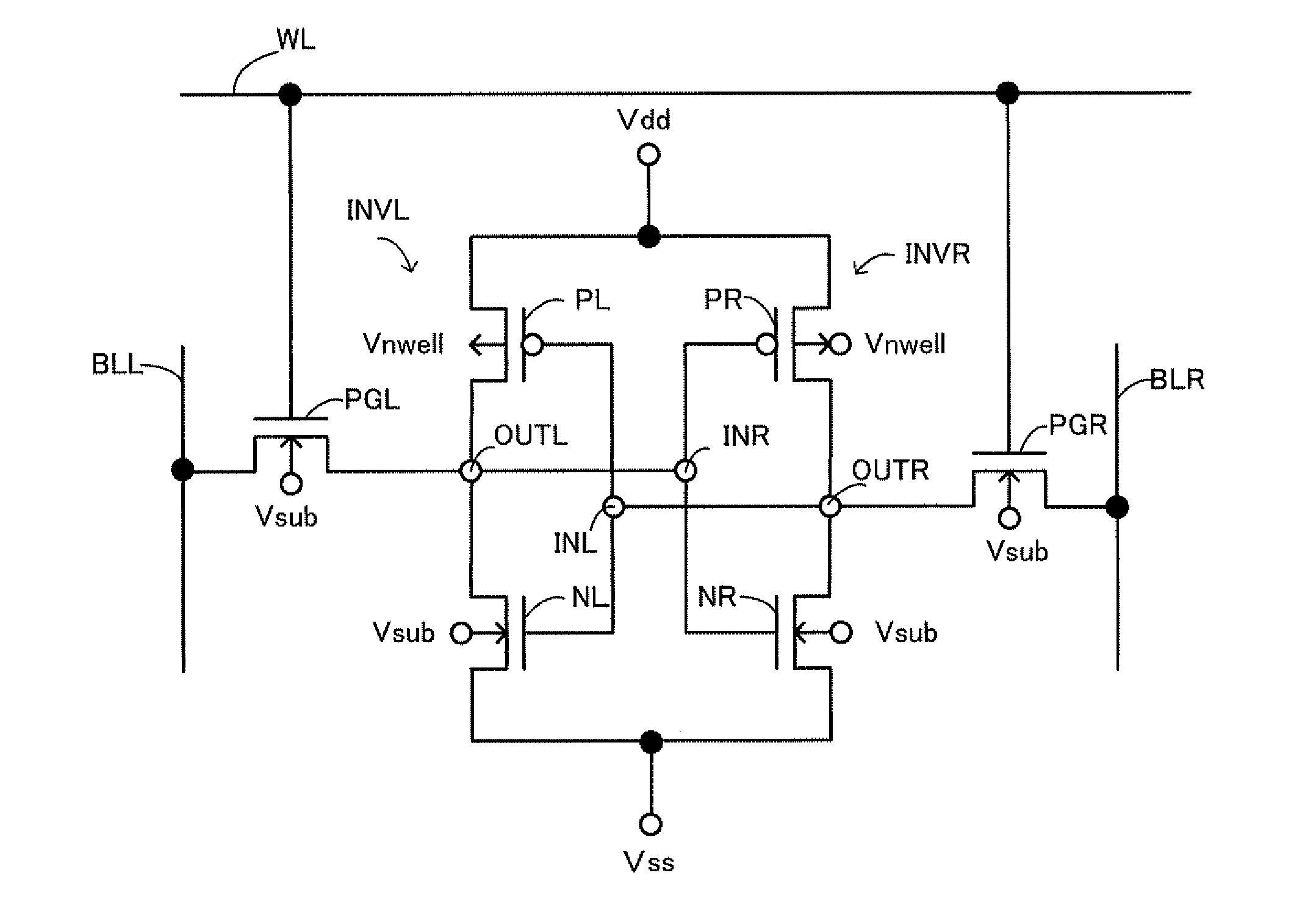
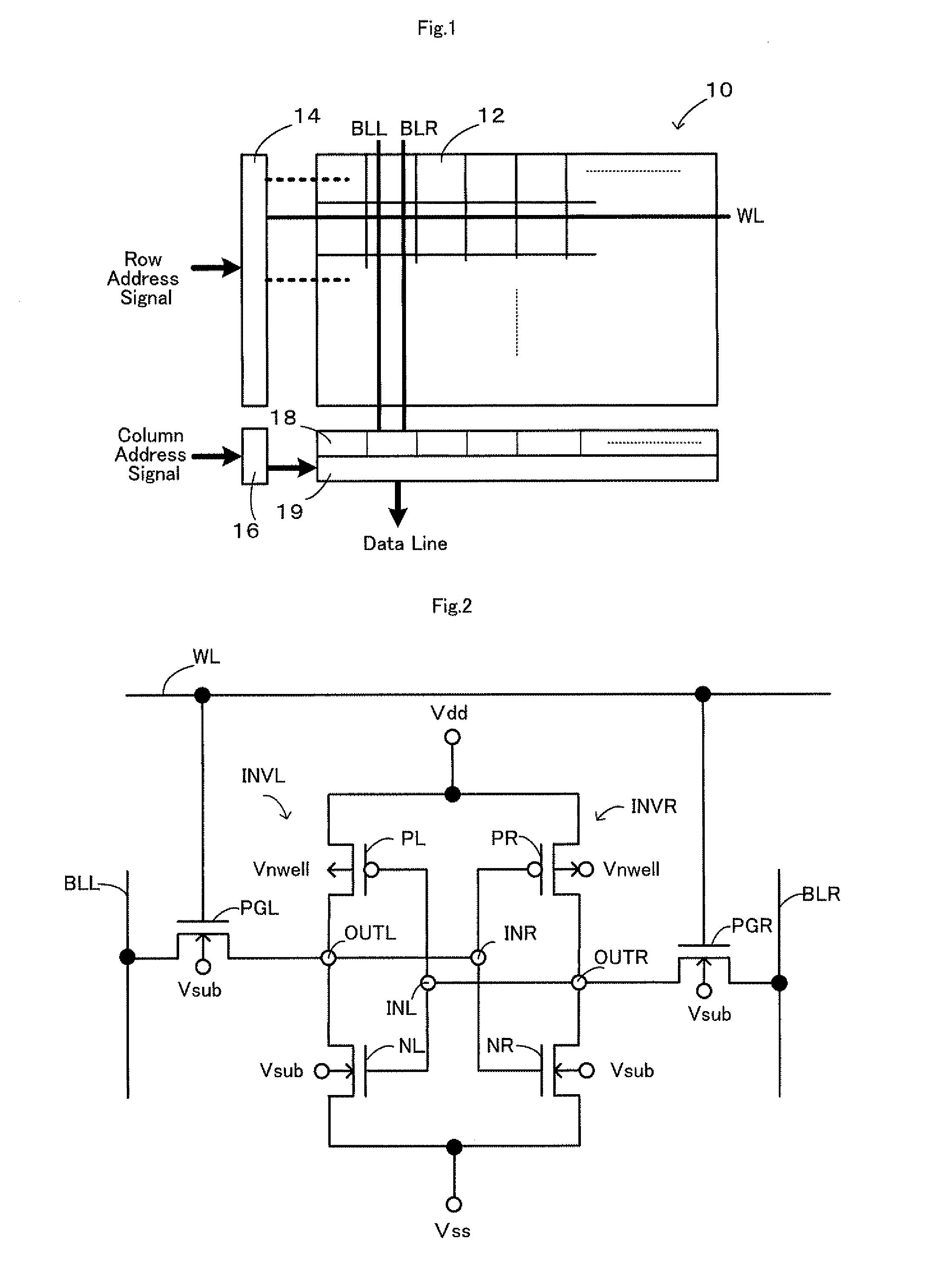
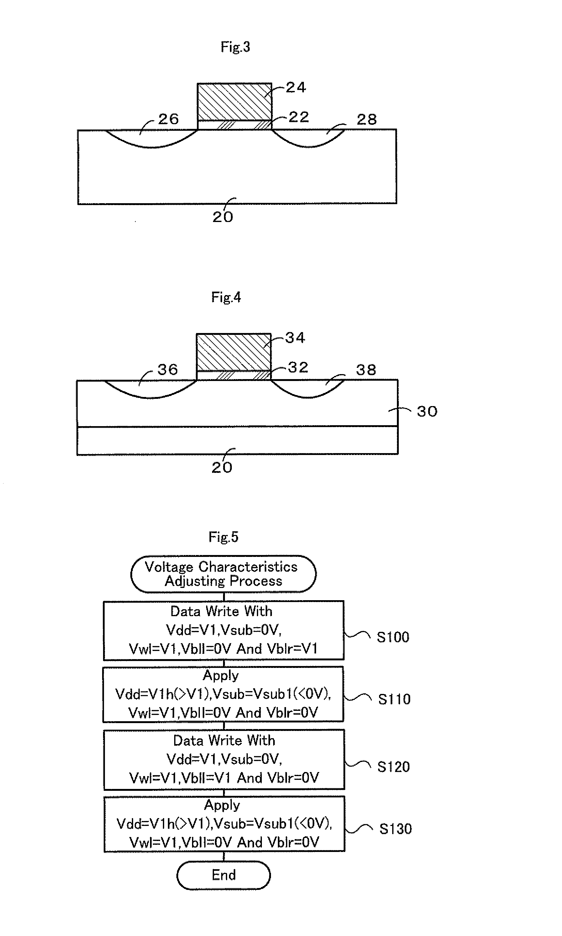
[0055]FIG. 1 is a diagram schematically illustrating a configuration of an SRAM (Statistic Random Access Memory) including a plurality of memory cells whose voltage characteristics are to be adjusted by a voltage characteristics adjusting method of the present invention. The SRAM 10 includes a plurality of memory cells 12 connected to a plurality of word lines WL and a plurality of bit lines BLL, BLR arranged in a matrix, a row decoder 14 which selects a word line WL corresponding to a row address signal when the row address signal is provided, a column decoder 16 selecting a pair of bit lines BLL, BLR corresponding to a column address signal when the column address signal is provided, a plurality of sense amplifiers 18 amplifying signals output from memory cells 12 to bit lines BLL, BLR, and a column select circuit 19 connecting selected bit lines BLL, BLR to a data line, not depicted, to which data is input and output. The memory cells 12 arranged in a row are connected to the sam...

second embodiment

[0073]According to the method for adjusting the voltage characteristics of the SRAM 10 of the second embodiment described above, the write characteristics of the memory cells 12 can be improved in a simplified way by forcing the voltage difference between the supply voltage application point Vdd and the bit lines BLL, BLR to a value V4 greater than the normal voltage difference V1 and forcing the voltage difference between the word line WL and the bit lines BLL, BLR to a value (V1+Vwll) greater than the normal voltage difference V1. Furthermore, by performing the processing at step S100 before the processing at step 110B, selection between the pass gate transistors PGL and PGR to inject holes into the insulating layer can be made, therefore the operating characteristics can be improved more properly.

[0074]While steps S100 and S100B are performed to adjust the threshold voltage of the pass gate transistor PGR and then the steps S120 and S130B are performed to adjust the threshold vol...

third embodiment

[0079]According to the method for adjusting the voltage characteristics of the SRAM 10 of the third embodiment described above, while voltages are being applied to the semiconductor substrate 20 of the memory cells 12, the word line WL and the bit lines BLL, BLR so that all of the substrate voltage Vsub, the word line voltage Vwl, and the bit line voltages Vbll, Vblr become 0 V, a voltage is applied to the supply voltage application point Vdd to change the voltage Vdd from 0 V to a value V2 that is lower than value V1. Then a voltage is applied to the word line WL so that the word line voltage Vw1 takes value V1, and a data read is performed. Then, voltages are applied to the supply voltage application points Vdd of the memory cells of the SRAM 10, the semiconductor substrate 20, the word line WL, and the bit lines BLL, RLR so that the voltage Vdd takes value V1h, the substrate voltage Vsub takes value Vsubl that is lower than 0 V, the word line voltage Vwll takes value V1, and the ...


PUM


Abstract

Voltages are applied to supply voltage application points of memory cells of an SRAM, a semiconductor substrate, a word line and bit lines so that voltage Vdd takes value V1, substrate voltage Vsub becomes 0 V, word line voltage Vw1 takes value V1, bit line voltage Vbll becomes 0 V, and bit line voltage Vblr takes value V1, the voltage difference between the word line and one of the bit lines is forced to be equal to a voltage difference V1h higher than a normal voltage difference V1 and the voltage difference between the word line and the other bit line is forced to be equal the normal voltage difference V1 lower than the voltage V1h to inject electrons into an insulating layer near a diffusion layer connected to an output terminal of an inverter constituting the memory cell. This can improve the operating characteristics of the memory cell.

Description

TECHNICAL FIELD[0001]The present invention relates to a method for adjusting voltage characteristics of a semiconductor element, a method for adjusting voltage characteristics of a semiconductor memory device, and a charge pump and a method for adjusting voltage characteristics of a charge pump.BACKGROUND ART[0002]A method for adjusting voltage characteristics of semiconductor memory devices of this type has been proposed in the past in which two halo regions having different peak impurity concentrations are formed between the source and drain of an insulted gate transistor making up a semiconductor memory device. A semiconductor memory device has been proposed in which this method is applied to a semiconductor device which an SRAM (Static Random Access Memory) cell having two inverters forming a latch and two access transistors, each of whose source or drain is connected to the output of the two inverters (see Non Patent Literature 1, for example). Two halo regions having different...

Claims


Application Information

Patent Timeline
Patent Type & Authority Applications(United States)
IPC IPC(8): G11C5/14G11C7/10G05F1/10
CPCH01L27/1104G11C5/145G11C7/1096G05F1/10G11C5/14G11C11/413H10B10/12
Inventor TAKEUCHI, KENMIYAJI, KOSUKETANAKAMARU, SHUHEIHONDA, KENTARO
Owner SEMICON TECH ACADEMIC RES CENT
Learn More