Localized, In-Vacuum Modification of Small Structures

a small structure and electrochemical technology, applied in the field of nanotechnology, can solve the problems of not working exactly as expected, often not solving problems, and often taking weeks or months to have the re-designed device produced, so as to improve the control of liquid dispensation, quickly and precisely deposit metal conductors, and remove metals or other conductive materials from structures

Active Publication Date: 2013-03-21
FEI CO
View PDF5 Cites 15 Cited by
  • Summary
  • Abstract
  • Description
  • Claims
  • Application Information

AI Technical Summary

Benefits of technology

[0012]Embodiments of the invention use a localized charge transfer mechanism to precisely deposit or remove material onto a substrate. In some embodiments, the invention can rapidly and precisely deposit metal conductors or rapidly remove metals o...

Problems solved by technology

When a new nanoscopic device is first produced in a fabrication facility, the design typically does not operate exactly as expected.
Due to the complexity of lithography processes typically used to fabricate microstructures, it typically takes weeks or months to have the re-designed device produced.
Further, the changes implemented frequently do not solve the problem, or the changes expose another flaw in the design requiring additional design changes.
The process of testing, re-designing and re-fabrication can significantly lengthen the time to market new semiconductor devices.
It is often difficult to obtain high purity materials using direct write deposition, primarily due to the incorporation into the deposit of other components of the precursor molecules or the elements from the incident ion beam, such as gallium ions.
This lack of control of co...

Method used


Image

  • Localized, In-Vacuum Modification of Small Structures
  • Localized, In-Vacuum Modification of Small Structures
  • Localized, In-Vacuum Modification of Small Structures

Examples


Embodiment Construction

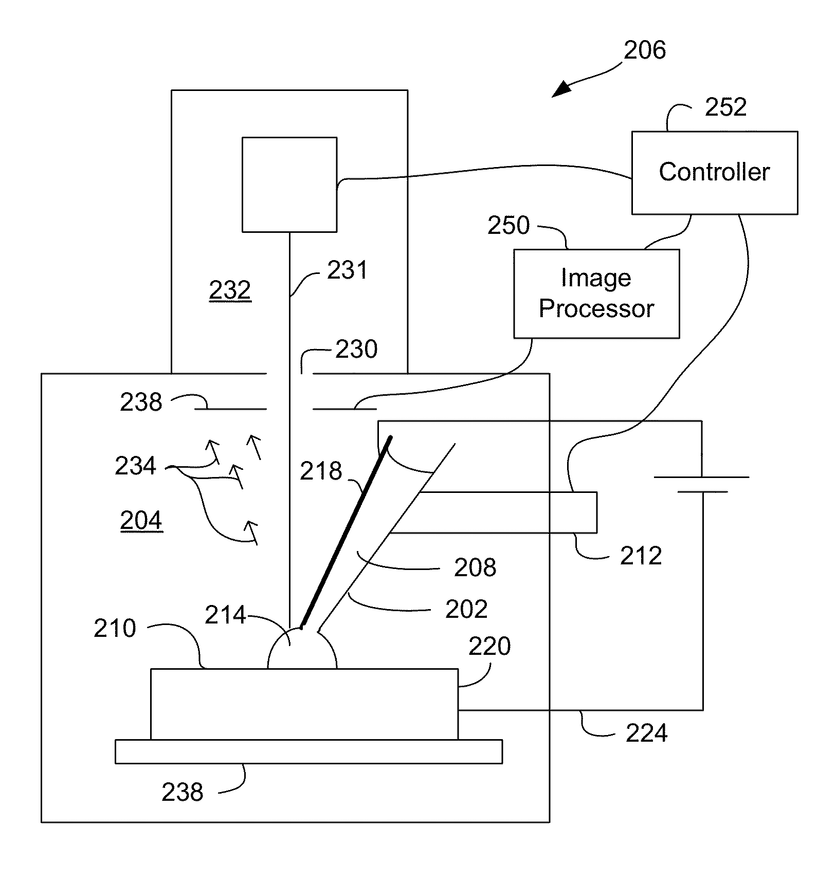
[0038]In a preferred embodiment, the present invention provides a means to directly deposit or etch conductive material onto a substrate. A nano pen dispenses an electrolyte and an electric current through the electrolyte electrochemically deposits material onto the surface or etches material from the surface. A “nano pen,” as used herein, comprises a device that dispenses small quantities of liquid to “write” or “etch” upon a substrate as the pen moves relative to the surface. Nano pens can comprise, for example, nanocapillaries, nano syringes, nanopipettes, etc.

[0039]Some embodiments of the invention can be used to deposit metals that are substantially pure. Because the metals are pure, they can have resistivities that are forty or more times lower than the resistivities of existing FIB-induced deposition of tungsten and platinum materials, and ten times lower than the resistivity of FIB-induced deposition of copper conductive materials. The resistivities are comparable to those o...


PUM

PropertyMeasurementUnit
Diameteraaaaaaaaaa
Diameteraaaaaaaaaa
Diameteraaaaaaaaaa

Abstract

A charge transfer mechanism is used to locally deposit or remove material for a small structure. A local electrochemical cell is created without having to immerse the entire work piece in a bath. The charge transfer mechanism can be used together with a charged particle beam or laser system to modify small structures, such as integrated circuits or micro-electromechanical system. The charge transfer process can be performed in air or, in some embodiments, in a vacuum chamber.

Description

TECHNICAL FIELD OF THE INVENTION[0001]The present invention relates to modifying small structures using localized electrochemistry and is particularly useful in the field of nanotechnology.BACKGROUND OF THE INVENTION[0002]Micrometer and nanometer scale structures are used in many fields including biological sciences, microelectromechanical systems (MEMS) and semiconductor manufacturing. For example, semiconductor devices such as microprocessors can be made up of millions of transistors, each interconnected by thin metallic lines branching on several levels and electrically isolated from each other by layers of insulating materials. Biological sensors may include microscopic regions of biological material that detect an analyte, transducers and electronics that provide an interpretable detectable signal.[0003]When a new nanoscopic device is first produced in a fabrication facility, the design typically does not operate exactly as expected. It is then necessary for the engineers who d...

Claims


Application Information

Patent Timeline
IPC IPC(8): C23C14/46
CPCC25D5/026C25D17/004C25D5/003C25D5/04C25D5/02C25D17/005C25D17/12C25D21/04C25D21/12C25D17/10H01J37/18H01J37/20H01J37/222H01J37/28H01J2237/182H01J2237/2003H01J2237/202H01J2237/2801
Inventor BOTMAN, AURELIEN PHILIPPE JEAN MACLOUTOTH, MILOSRANDOLPH, STEVENNARUM, DAVID H.
Owner FEI CO
Why Eureka
Try Eureka