
Integrated Circuit and Sensor for Imaging

a technology applied in the field of integrated circuits and sensors for imaging, can solve the problems of inability to read out conventional discrete or hybrid electronics, lack of good quantum efficiency of inability to achieve high-energy x-rays and gamma rays, etc., to achieve fast trigger output, low noise, and the effect of handling large rates

Inactive Publication Date: 2013-02-21
NOVA R&D
View PDF0 Cites 18 Cited by
  • Summary
  • Abstract
  • Description
  • Claims
  • Application Information

AI Technical Summary

Benefits of technology

The new RENA-2 ASIC is a flexible and easy-to-use design that can be used for a wide range of applications. It features low-noise performance, self-trigger capability, several different peaking times, and the daisy-chain option. The chip also includes user-selectable dynamic ranges, fast trigger output, and the ability to provide channel-by-channel time difference information. The design goal for noise performance is significantly improved over the present RENA chip and substantial innovation was required to reach this goal. The new chip incorporates a pole zero cancellation circuit to handle large rates without significant pileup, and is tolerant to leakage current so that it can be used DC coupled. The new features include low noise, self resetting charge sensitive input amplifier, and fast trigger output for coincident event detection. The peaking times can be adjusted from about 0.4 to 40 microseconds, making the chip suitable for a wide range of detectors. The design is improved by eliminating unnecessary connections and interface. Overall, the new RENA ASIC is a significantly improved design that addresses different requirements for various applications.

Problems solved by technology

Although an excellent detector, silicon, with an atomic number (Z) of 14, does not have good quantum efficiency for higher energy x-rays and gamma rays.
Although strongly promising high-Z position sensitive solid state detectors were developed, an essential component to make them viable instruments for detecting and imaging x-rays, gamma rays and particles has been missing.
Such detectors have many channels with small pitch, and reading them out with conventional discrete or hybrid electronics is not a viable option.
1. They do not have a self trigger output. In high energy physics experiments, an external machine trigger is available to inform the data acquisition (DAQ) system about the exact time of an event for reading out the chips. In addition, the event trigger is typically based on the overall event topology rather than the signal levels in individual channels, which precludes its implementation on the readout chip.
2. The solid-state detectors for which these ASICs were developed provide position information only; the energy information is largely irrelevant as the particles of interest are all minimum ionizing. Consequently, such chips do not need to have low noise and thus high energy resolution capability.
Therefore, the application of position sensitive solid state detectors to nuclear and astrophysics and to medical and industrial imaging was largely delayed as a suitable ASIC readout chip was not available.
Also the RENA chip could only partially answer the requirements of many applications listed above.

Method used


Image

  • Integrated Circuit and Sensor for Imaging
  • Integrated Circuit and Sensor for Imaging
  • Integrated Circuit and Sensor for Imaging

Examples


Embodiment Construction

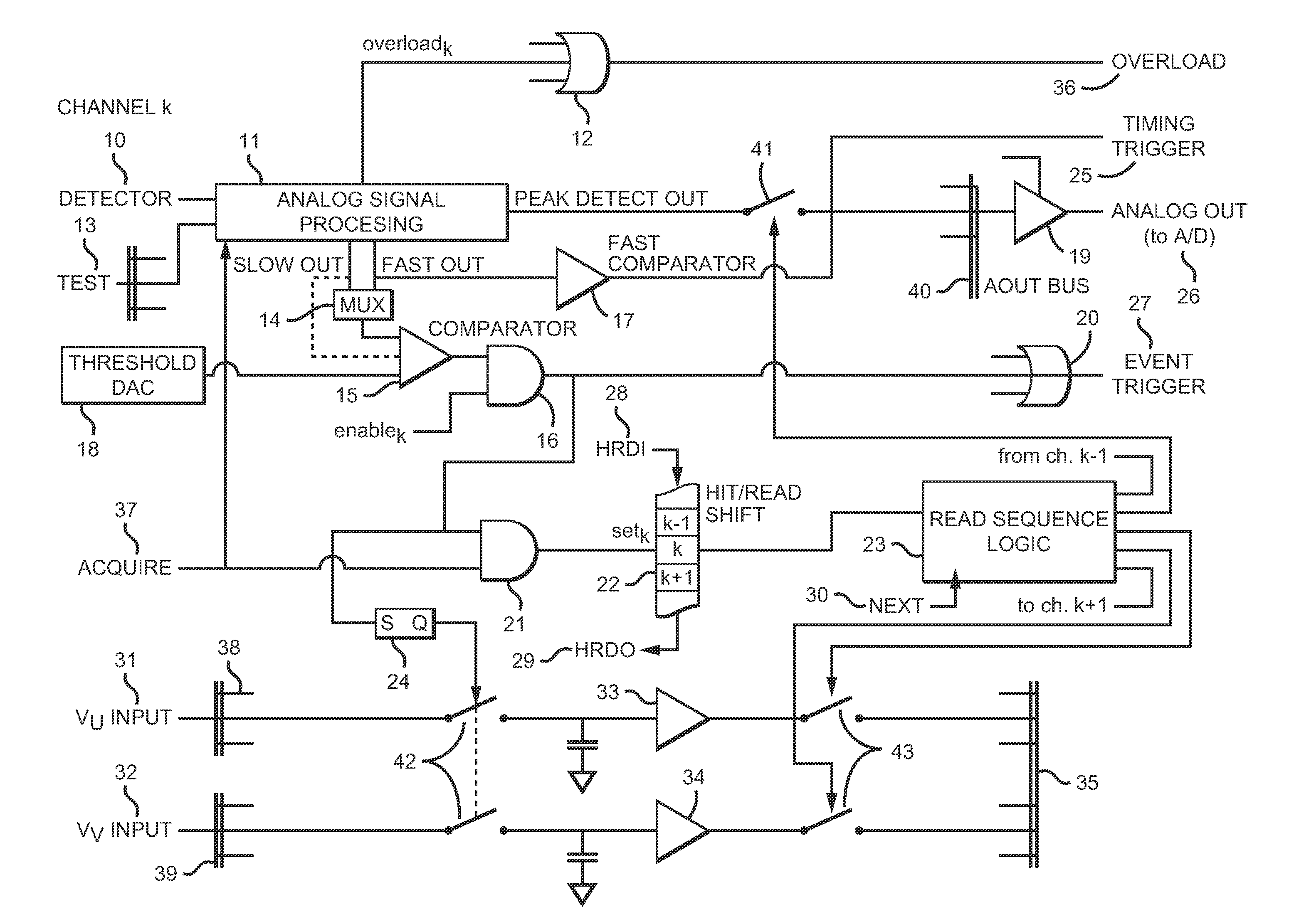
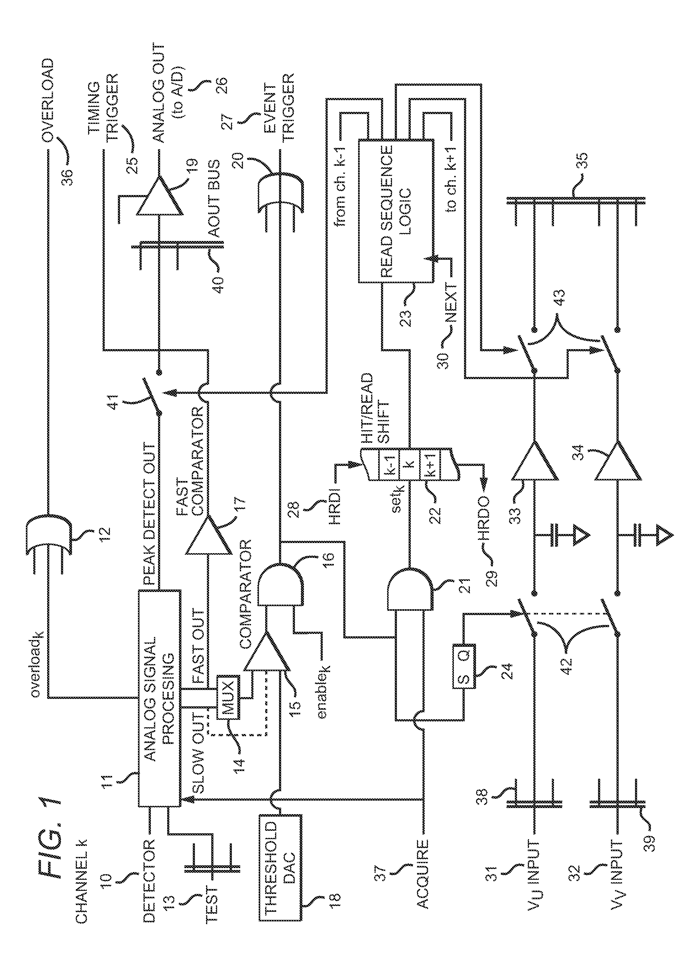
[0056]Referring to the ASIC described in FIG. 1 a detector 10 is connected to the input of the ASIC and the input goes to an analog signal processing unit 11. The FIG. 1 shows only one of the analog channels of the ASIC, the k channel. Analog processing unit is described below. Peak detector output of the analog signal processing unit 11 goes to analog output buffer amplifier 19 through a switch 41 controlled by read sequence logic 23. The peak detect output is also attached onto a bus 40 before it enters analog output buffer 19. Analog output is made available to the outside world as an output 26 of the ASIC. A test input 13 is used to test the analog signal processing unit. An overload sensing element 12 is connected to the analog signal processing unit 11. Output of the overload sensor 36 is provided to outside world as an output of the ASIC.

[0057]Analog signal processing unit 11 outputs a slow and fast shaper signal during processing of the signal from the detector 10 which go i...


PUM


Abstract

New sensors and different embodiments of multi-channel integrated circuit are provided. The new high energy and spatial resolution sensors use both solid state and scintillator detectors. Each channel of the readout chip employs low noise charge sensitive preamplifier(s) at its input followed by other circuitry. The different embodiments of the sensors and the integrated circuit are designed to produce high energy and / or spatial resolution two-dimensional and three-dimensional imaging for widely different applications. Some of these applications may require fast data acquisition, some others may need ultra high energy resolution, and a separate portion may require very high contrast. The embodiments described herein addresses all these issues and also other issues that may be useful in two and three dimensional medical and industrial imaging. The applications of the new sensors and integrated circuits addresses a broad range of applications such as medical and industrial imaging, NDE and NDI, security, baggage scanning, astrophysics, nuclear physics and medicine.

Description

[0001]This application is a divisional of co-pending U.S. application Ser. No. 10 / 378,664 filed Mar. 5, 2003, now issued U.S. Pat. No. 7,868,665, which claims the benefit of the filing date of U.S. Provisional Patent Application No. 60 / 361,330 filed Mar. 5, 2002, both of which are incorporated herein by reference. This application also references previous U.S. Pat. Nos. 5,696,458, 6,150,849 and 6,333,648 by the inventor, which are both incorporated herein by reference for all purposes.GOVERNMENT RIGHTS NOTICE[0002]This invention was made with U.S. Government support under Contract Numbers DAMD 17-98-8137, DAAE30-02-C-1015 and DAAE30-02-C-10270, which are awarded by Department of Defense. The U.S. Government has certain rights in the invention.FIELD OF THE INVENTION[0003]There is need for high spatial and energy resolution photonic sensors and integrated circuits (IC) are needed to produce imaging. Scintillation counters read out by individual photomultiplier tubes has limitations in...

Claims


Application Information

Patent Timeline
Patent Type & Authority Applications(United States)
IPC IPC(8): H04N5/335H04N25/00H03F3/08H03F3/45
CPCH03F3/087H03F2200/331H03F3/45475G01T1/171H04N25/773
Inventor TUMER, TUMAY O.CLAJUS, MARTINCALDERWOOD, ROBERT F.VISSER, GERARD
Owner NOVA R&D
Learn More