Portable electronic device, antenna structure, and antenna producing process thereof
a technology of electronic devices and antennas, applied in the direction of waveguide devices, radiating element structural forms, resonance antennas, etc., can solve the problem that the size of electronic devices cannot be further reduced, and achieve the effect of increasing the thickness of the antenna pattern and increasing the thickness
- Summary
- Abstract
- Description
- Claims
- Application Information
AI Technical Summary
Benefits of technology
Problems solved by technology
Method used
Image

Examples
first embodiment
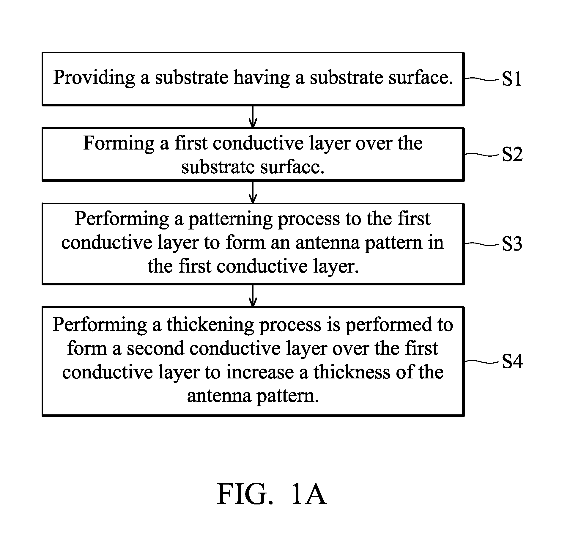
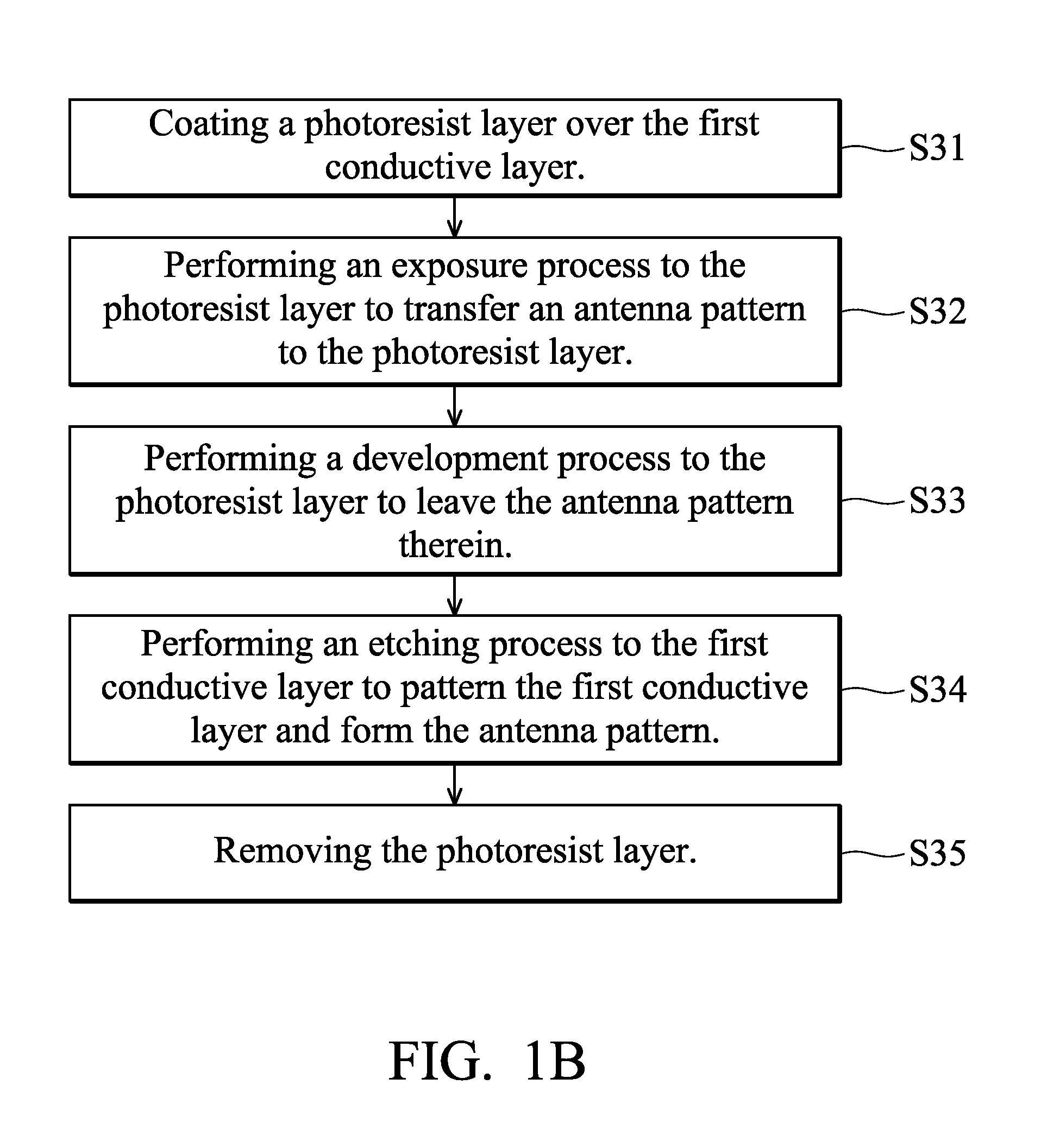
[0034]an antenna producing process comprises the main steps shown in FIG. 1A. First, a substrate is provided, having a substrate surface (S1). Next, a first conductive layer is formed over the substrate surface (S2). Next, a patterning process is performed to the first conductive layer to form an antenna pattern in the first conductive layer (S3). Then, a thickening process is performed to form a second conductive layer over the first conductive layer, thereby increasing a thickness of the antenna pattern and forming a first exemplary antenna structure.
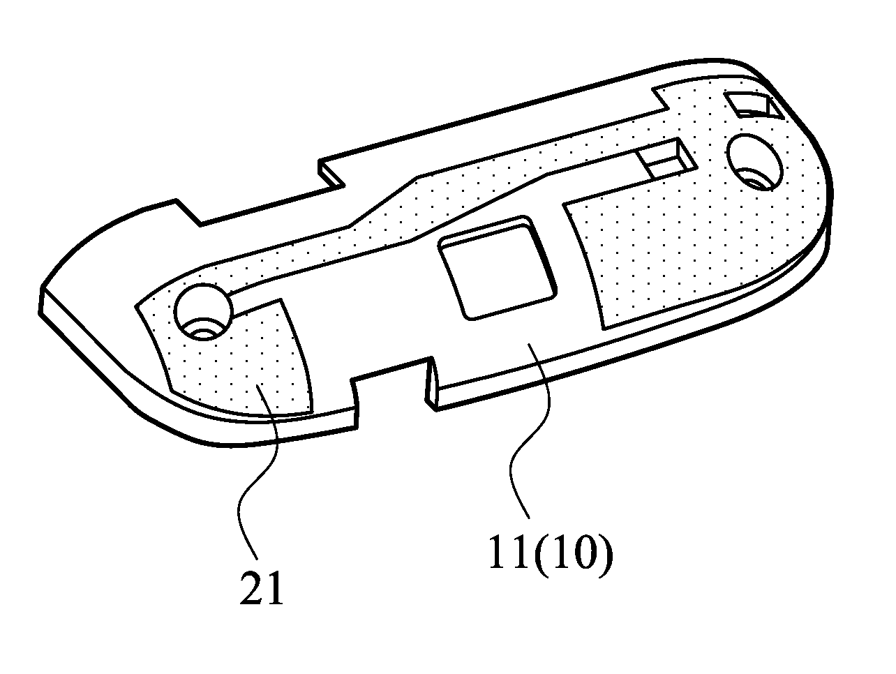
[0035]The substrate can be, for example, a case of a portable electronic device. The substrate surface can be an inner or outer surface of the portable electronic device. Referring to FIG. 2A, an exemplary substrate 10 is illustrated, having a substrate surface 11, and the substrate surface can be, for example, a curved surface.
[0036]In FIG. 3, the first embodiment of the antenna producing process is applied to form an antenna 21 over...
second embodiment
[0047]an antenna producing process comprises the main steps shown in FIG. 5A. First, a substrate is provided, having a substrate surface (S5). Next, a composite conductive layer is formed over the substrate surface (S6). Next, a patterning process is performed to the composite conductive layer to form an antenna pattern in the composite conductive layer (S7) and form the second exemplary antenna structure.
[0048]The substrate can be, for example, a case of a portable electronic device. The substrate surface can be an inner or outer surface of the portable electronic device. Referring to FIG. 2A, an exemplary substrate 10 is illustrated, having a substrate surface 11, and the substrate surface can be, for example, a curved surface.
[0049]In FIG. 3, the second embodiment of the antenna producing process is applied to form an antenna 21 over the substrate surface 11 of the substrate 10, such that a space occupied by the antenna 21 can be reduced to a minimum, and an inner space of the po...
third embodiment
[0058]an antenna producing process comprises the main steps shown in FIG. 7A. First, a substrate is provided, having a substrate surface (S8). Next, a first conductive layer and a photoresist layer are formed over the substrate surface (S9). Next, a patterning process is performed to the photoresist layer to form an opening therein, wherein the opening is formed with an antenna pattern that exposes a portion of the first conductive layer (S10). Next, a thickening process is performed to form a second conductive layer, thereby increasing a thickness of the portion of the first conductive layer exposed by the opening (S11). Next, the photoresist layer is removed, and the portion of the first conductive layer without an increased thickness is removed by using the second conductive layer formed over the portion of the first conductive layer as an etching mask, thereby obtaining an antenna structure (S12).
[0059]The substrate can be, for example, a case of a portable electronic device. Th...
PUM
| Property | Measurement | Unit |
|---|---|---|
| Thickness | aaaaa | aaaaa |
| Electrical conductor | aaaaa | aaaaa |
Abstract
Description
Claims
Application Information
 - R&D
- Intellectual Property
- Life Sciences
- Materials
- Tech Scout
- Unparalleled Data Quality
- Higher Quality Content
- 60% Fewer Hallucinations
Browse by: Latest US Patents, China's latest patents, Technical Efficacy Thesaurus, Application Domain, Technology Topic, Popular Technical Reports.
© 2025 PatSnap. All rights reserved.Legal|Privacy policy|Modern Slavery Act Transparency Statement|Sitemap|About US| Contact US: help@patsnap.com