
Integrated circuit comprising scan test circuitry with controllable number of capture pulses

a scan test circuit and integrated circuit technology, applied in the direction of logical operation testing, instruments, measurement devices, etc., can solve the problems of inability to test the functional address and data path, inability to provide test coverage, and inability to control the compression level

Inactive Publication Date: 2012-12-27
AVAGO TECH INT SALES PTE LTD
View PDF11 Cites 18 Cited by
  • Summary
  • Abstract
  • Description
  • Claims
  • Application Information

AI Technical Summary

Benefits of technology

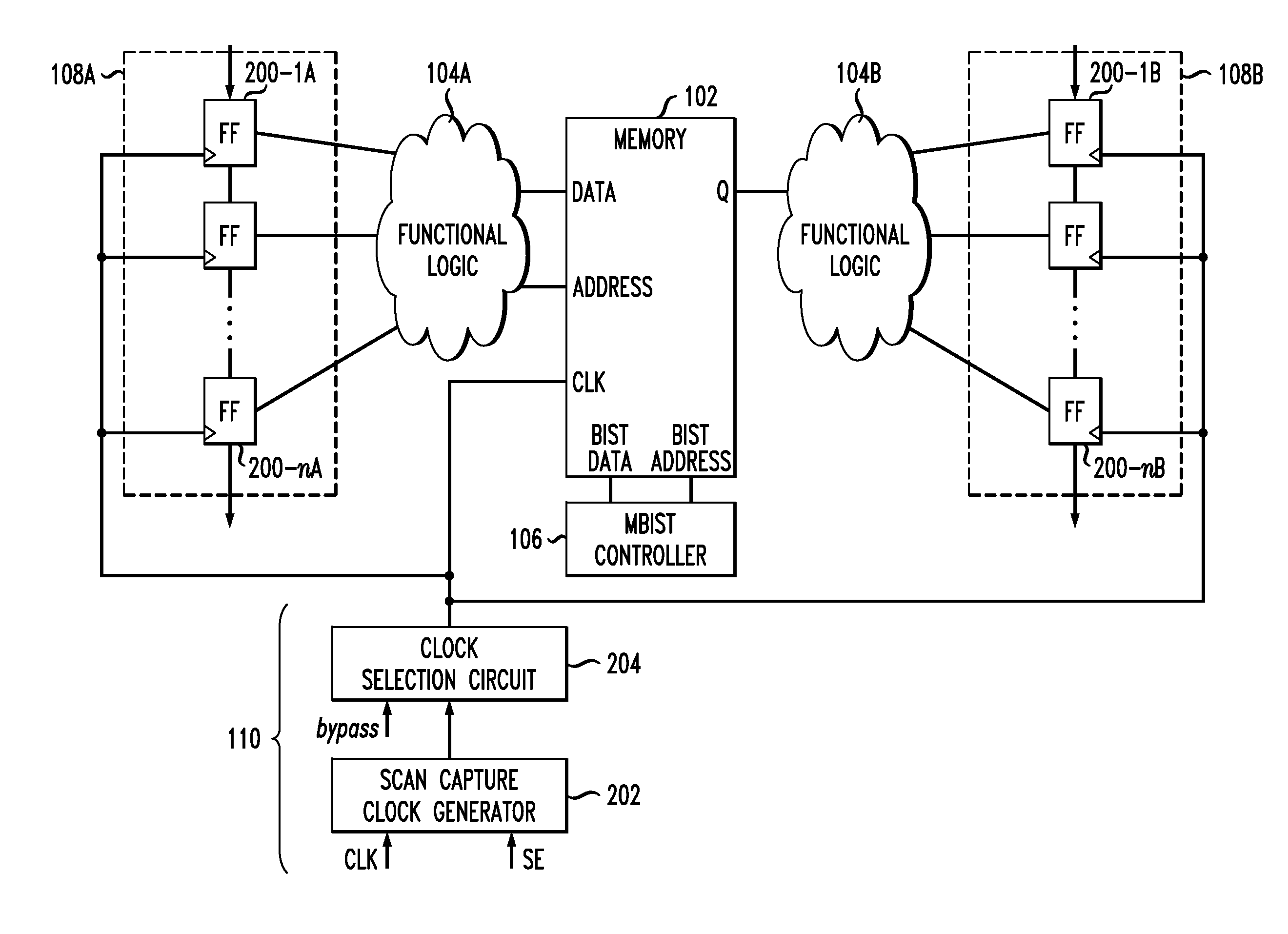
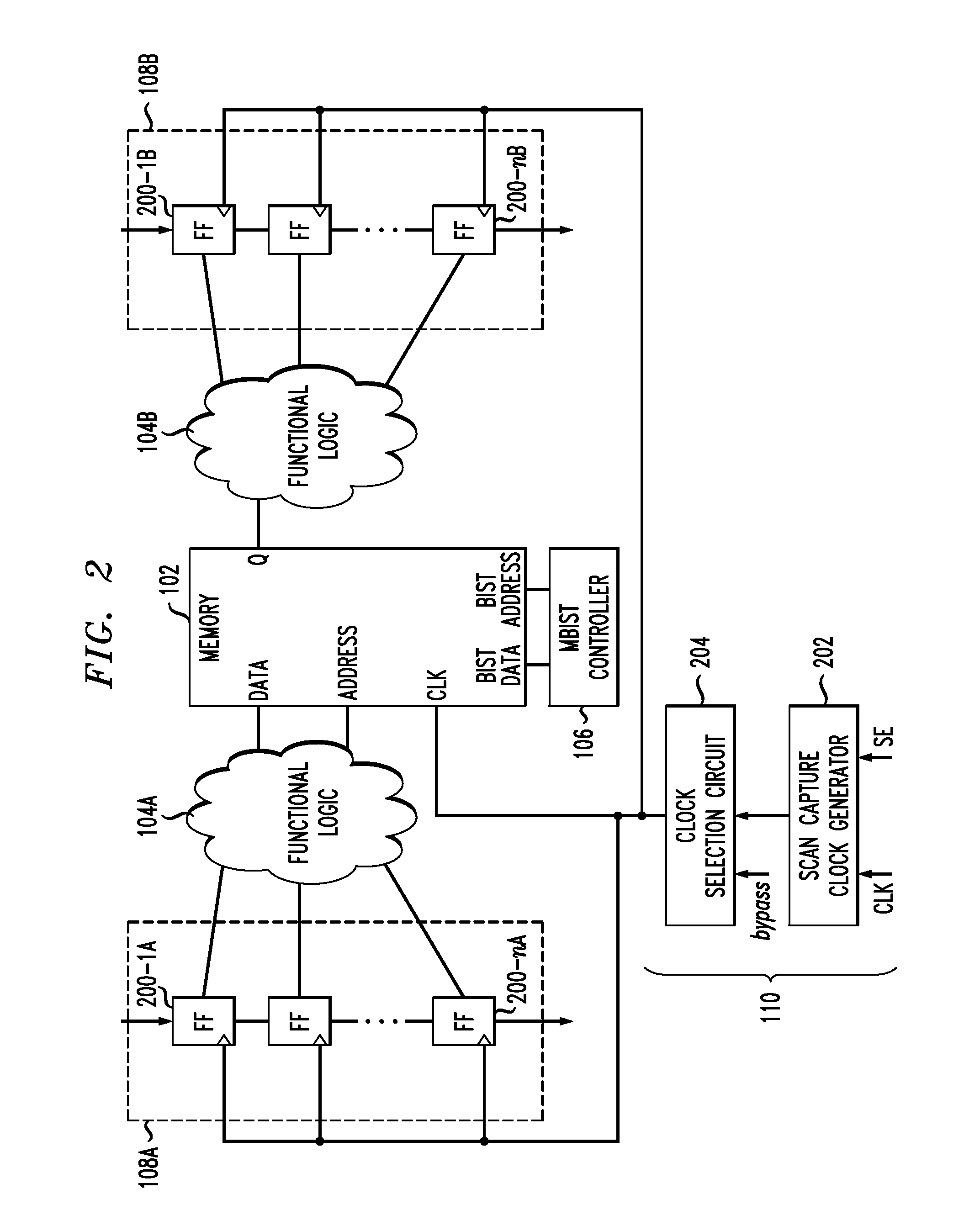
[0006]Illustrative embodiments of the invention provide improved circuitry and techniques for scan testing of integrated circuits. For example, in one or more such embodiments, an integrated circuit comprises an embedded memory and an associated MBIST controller, and is further configured to include scan test circuitry that generates a scan capture clock in which the number of capture pulses can be controlled in real time based on test patterns being applied to scan chains of the integrated circuit. The variable number of capture pulses facilitates testing of sequential logic or other functional logic that is not covered by the MBIST testing functionality of the integrated circuit, such as functional address and data paths of the embedded memory that are bypassed during MBIST testing.
[0009]The illustrative embodiments provide considerable advantages over conventional arrangements. For example, a given such embodiment can provide a variable number of capture pulses for supporting at-speed scan testing of functional paths through an embedded memory that are bypassed during conventional MBIST testing of the embedded memory. The number of capture pulses generated can be varied in real time based on each test pattern to be applied during the at-speed scan testing.

Problems solved by technology

However, the use of high levels of scan compression can adversely impact diagnostic resolution, that is, the ability to attribute a particular failure to an exact fault or set of faults within the combinational logic.
As a result, when using scan compression, a tradeoff exists between compression level and diagnostic resolution.
A significant problem with existing techniques for MBIST testing of embedded memory in an integrated circuit is that there is typically certain sequential logic or other functional logic at the input or output of the memory that is not covered by the MBIST testing.
For example, during MBIST testing the functional address and data paths going into the embedded memory are usually bypassed and an MBIST controller instead provides the address and data inputs for the memory array being tested, which unfortunately provides no test coverage for the functional address and data paths.
Similar test coverage problems can arise in other types of integrated circuits.

Method used


Image

  • Integrated circuit comprising scan test circuitry with controllable number of capture pulses
  • Integrated circuit comprising scan test circuitry with controllable number of capture pulses
  • Integrated circuit comprising scan test circuitry with controllable number of capture pulses

Examples


Embodiment Construction

[0016]The invention will be illustrated herein in conjunction with exemplary integrated circuits comprising scan test circuitry for supporting scan testing of other internal circuitry of those integrated circuits. It should be understood, however, that the invention is more generally applicable to any integrated circuit in which it is desirable to provide improved testing of functional logic associated with an embedded memory or other internal circuitry of the integrated circuit. For example, the disclosed techniques can be adapted for application to testing of integrated circuits that comprise stand-alone memory devices, such as RAM, ROM or Flash memory integrated circuits, which may additionally or alternatively include multi-level memory integrated circuits.

[0017]FIG. 1 shows an integrated circuit 100 that comprises an embedded memory 102 and associated functional logic 104. An MBIST controller 106 is coupled to embedded memory 102 for performing conventional MBIST testing of the...


PUM


Abstract

An integrated circuit comprises scan test circuitry and additional circuitry subject to testing utilizing the scan test circuitry. The scan test circuitry comprises a plurality of scan chains coupled to the additional circuitry, a scan capture clock generator configured to generate a scan capture clock signal having a controllable number of capture pulses, and a clock selection circuit configured to select between at least the scan capture clock signal and a scan shift clock signal for application to clock signal inputs of the scan chains. In one embodiment, the scan capture clock generator comprises a finite state machine, a plurality of capture clock pulse circuits each generating a capture clock pulse signal comprising a different number of capture clock pulses, and logic circuitry coupled to the finite state machine and having inputs adapted to receive the outputs of the capture clock pulse circuits. The logic circuitry is configured to provide at an output thereof at least a portion of a particular one of the capture clock pulse signals based on a current state of the finite state machine.

Description

FIELD OF THE INVENTION[0001]The present invention relates generally to integrated circuit testing, and more particularly to integrated circuit testing using scan test circuitry.BACKGROUND OF THE INVENTION[0002]Integrated circuits are often designed to incorporate scan test circuitry that facilitates testing for various internal fault conditions. Such scan test circuitry typically comprises scan chains, which are chains of flip-flops that are used to form serial shift registers for applying test patterns at inputs to combinational logic of the integrated circuit and for reading out the corresponding results.[0003]As integrated circuits have become increasingly complex, scan compression techniques have been developed which reduce the number of test patterns that need to be applied when testing a given integrated circuit, and therefore also reduce the required test time. However, the use of high levels of scan compression can adversely impact diagnostic resolution, that is, the ability...

Claims


Application Information

Patent Timeline
IPC IPC(8): G01R31/3177G06F11/25
CPCG01R31/318594G01R31/318552
Inventor TEKUMALLA, RAMESH C.
Owner AVAGO TECH INT SALES PTE LTD
Learn More