Chip package with reinforced positive alignment features

a technology of positive alignment and chip package, which is applied in the field of chip package, can solve the problems of increasing the difficulty of existing interconnects providing suitable communication characteristics, high bandwidth, reliability and low cost, and the difficulty of bonding chips to each other and to carriers (such as printed circuit boards) in chip stacks, so as to facilitate mechanical alignment, increase the shear strength, and facilitate the alignment between the substrate and the second substrate

Active Publication Date: 2012-12-27
ORACLE INT CORP
View PDF1 Cites 5 Cited by
  • Summary
  • Abstract
  • Description
  • Claims
  • Application Information

AI Technical Summary

Benefits of technology

[0011]One embodiment of the present disclosure provides a chip package that includes a substrate having a positive feature defined on a surface of the substrate, where the positive feature protrudes above a region on the surface proximate to the positive feature. Furthermore, the chip package includes a mechanical reinforcement mechanism defined on the substrate proximate to the positive feature that increases the shear strength of the positive feature relative to the substrate.
[0015]Another embodiment provides the MCM that includes the chip package. This MCM may include a second substrate, where the positive feature facilitates mechanical alignment between the substrate and the second substrate. For example, the second substrate may include a negative feature defined on a second surface of the second substrate. This negative feature may be recessed below a region on the second surface proximate to the negative feature, and the positive feature may mate with the negative feature.
[0016]Alternatively or additionally, the second substrate may include a second positive feature defined on a second surface of the second substrate, where the second positive feature protrudes above a region on the second surface proximate to the second positive feature. Moreover, the second substrate may include a second mechanical reinforcement mechanism defined on the second substrate proximate to the second positive feature, where the second mechanical reinforcement mechanism increases the shear strength of the second positive feature relative to the second substrate. Furthermore, alignment between the substrate and the second substrate may be facilitated by the positive feature and the second positive feature.
[0017]Another embodiment provides a method for increasing the shear strength in the chip package. During this method, the positive feature is defined on the surface of the substrate in the chip package, where the positive feature protrudes above the region on the surface proximate to the positive feature. Then, the mechanical reinforcement mechanism is fabricated on the substrate proximate to the positive feature, where the mechanical reinforcement mechanism increases the shear strength of the positive feature relative to the substrate.

Problems solved by technology

As integrated-circuit (IC) technology continues to scale to smaller critical dimensions, it is increasingly difficult for existing interconnects to provide suitable communication characteristics, such as: high bandwidth, low power, reliability and low cost.
However, it is difficult to bond chips to each other and to carriers (such as printed circuit boards) in chip stacks using existing assembly techniques because of stringent requirements for alignment accuracy and manufacturing throughput.
However, it typically involves multiple assembly operations, which makes assembly of the chip package complicated, time-consuming and expensive.
In addition, fabricating the positive and / or negative features can be challenging.
However, many subtractive fabrication processes are incompatible with other semiconductor fabrication processes or may interfere with the function of a semiconductor wafer.
However, because of poor adhesion to the substrates in the chips, the resulting ‘additive’ features often fail when subjected to lateral shear forces, such as those associated with different coefficients of thermal expansion and lateral misalignment of the chips in the MCM.
Consequently, additive features are often unreliable, which can prevent them from properly aligning the chips in the MCM.

Method used


Image

  • Chip package with reinforced positive alignment features
  • Chip package with reinforced positive alignment features
  • Chip package with reinforced positive alignment features

Examples


Embodiment Construction

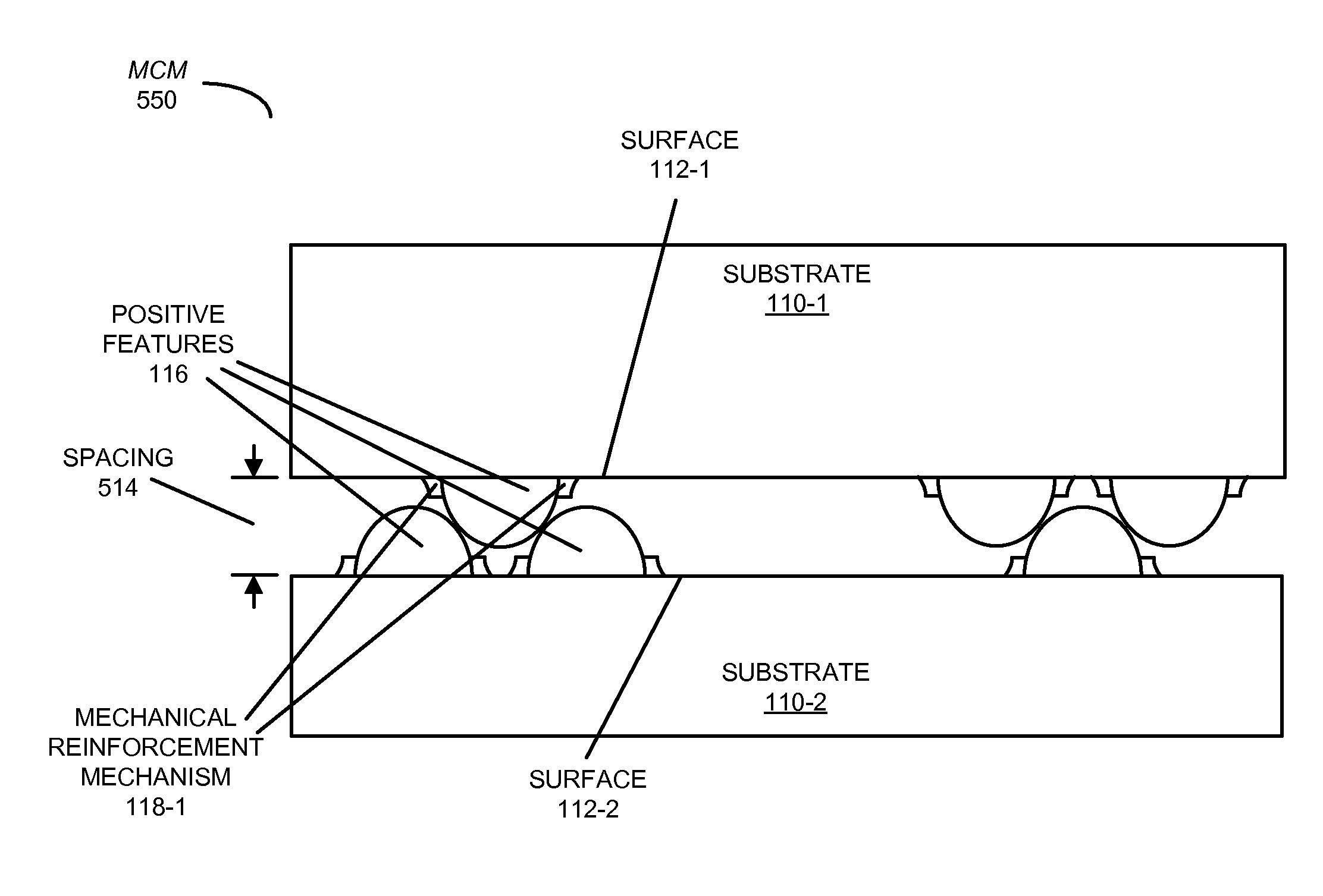
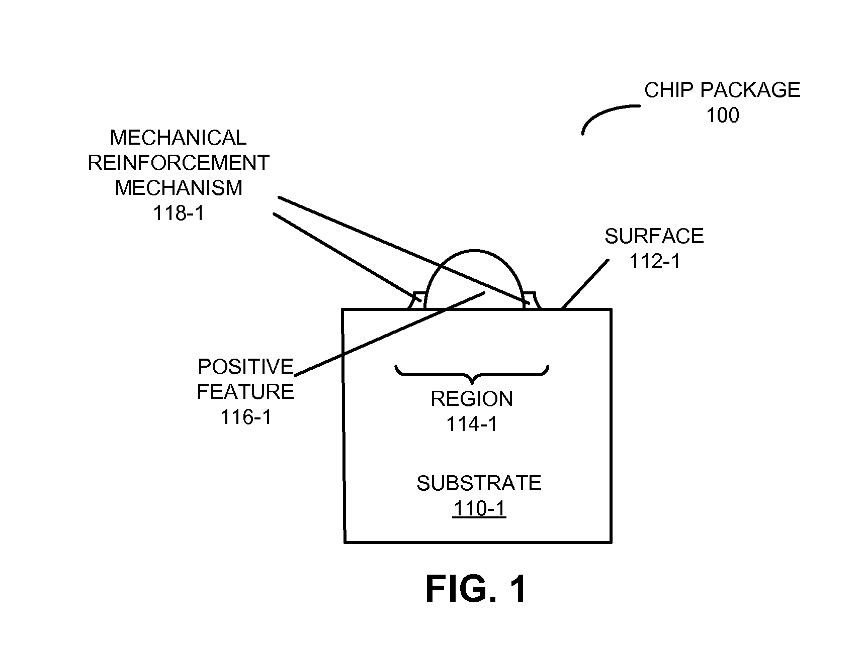
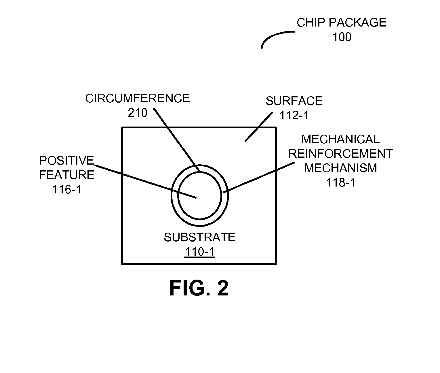
[0027]Embodiments of a chip package, a multi-chip module (MCM) that includes the chip package, an electronic device that includes the MCM, and a technique for increasing a lateral shear strength of the chip package are described. This chip package includes a substrate having a positive feature, which is defined on a surface of the substrate and which protrudes above a region on the surface proximate to the positive feature. Furthermore, the chip package includes a mechanical reinforcement mechanism defined on the substrate proximate to the positive feature that increases the shear strength of the positive feature relative to the substrate (and, more generally, the structural integrity of the positive features). In this way, the chip package may facilitate increased reliability of the MCM that includes the chip package.

[0028]By increasing the reliability of the MCM, the chip package may increase the yield of the MCM. Furthermore, the chip package may be used to: accurately align comp...


PUM

PropertyMeasurementUnit
thickaaaaaaaaaa
thickaaaaaaaaaa
bondline heightaaaaaaaaaa

Abstract

A chip package includes a substrate having a positive feature, which is defined on a surface of the substrate and which protrudes above a region on the surface proximate to the positive feature. Furthermore, the chip package includes a mechanical reinforcement mechanism defined on the substrate proximate to the positive feature that increases a lateral shear strength of the positive feature relative to the substrate. In this way, the chip package may facilitate increased reliability of a multi-chip module (MCM) that includes the chip package.

Description

GOVERNMENT LICENSE RIGHTS[0001]The United States Government has a paid-up license in this invention and the right in limited circumstances to require the patent owner to license others on reasonable terms as provided for by the terms of Agreement No. HR0011-08-9-0001 awarded by the Defense Advanced Research Projects Administration.BACKGROUND[0002]1. Field[0003]The present disclosure generally relates to a chip package for semiconductor dies or chips. More specifically, the present disclosure relates to a chip package that includes mechanically reinforced positive features that facilitate alignment of semiconductor chips in a multi-chip module (MCM) that includes the chip package.[0004]2. Related Art[0005]As integrated-circuit (IC) technology continues to scale to smaller critical dimensions, it is increasingly difficult for existing interconnects to provide suitable communication characteristics, such as: high bandwidth, low power, reliability and low cost. Engineers and researchers...

Claims


Application Information

Patent Timeline
Patent Type & Authority Applications(United States)
IPC IPC(8): H01L23/48B32B3/00
CPCH01L2224/13655Y10T428/24479H01L24/13H01L2224/16145H01L2224/81141H01L2224/1319H01L2224/13609H01L2224/81193H01L23/48H01L2224/81815H01L2224/10126H01L2224/131H01L2224/13671H01L24/16H01L2224/81855H01L2224/81194H01L2224/1357H01L24/81H01L2224/81097H01L2224/13611H01L2924/00014H01L2924/014H01L2924/00012H01L2924/01079H01L2924/01029H01L2924/01028H01L2924/01082H01L2924/0105H01L2224/16105
Inventor KRISHNAMOORTHY, ASHOK V.STEPHEN, CRAIG A.CUNNINGHAM, JOHN E.MITCHELL, JAMES G.
Owner ORACLE INT CORP
Why Eureka
Try Eureka