Tiled electro-optic imaging device

a technology of electro-optic imaging and tiles, which is applied in the direction of radiation controlled devices, optical radiation measurement, identification means, etc., can solve the problems of requiring re-adjustment, affecting the appearance of tiles, so as to facilitate the mechanical alignment of tiles, reduce the visibility of tile seams, and increase the apparent uniformity of tiles

Inactive Publication Date: 2005-04-19
GLOBAL OLED TECH
View PDF17 Cites 43 Cited by
  • Summary
  • Abstract
  • Description
  • Claims
  • Application Information

AI Technical Summary

Benefits of technology

[0007]The present invention has the advantage that it decreases the visibility of tile seams, increases the apparent uniformity of the tiles, and facilitates the mechanical alignment of the tiles in the electro-optic imaging device.

Problems solved by technology

However, construction of tiled imaging devices is difficult.
There are calibration techniques by which the uniformity and color balance of a display or image sensor tile can be adjusted, but these are difficult, require re-adjustment over time, and are often inadequate.
The assembly of flat-panel tiles is also a problem.
This process is expensive and slow and products are prone to fall out of alignment over time without expensive forms or brackets to align the tiles once they are placed.

Method used


Image

  • Tiled electro-optic imaging device
  • Tiled electro-optic imaging device
  • Tiled electro-optic imaging device

Examples


Embodiment Construction

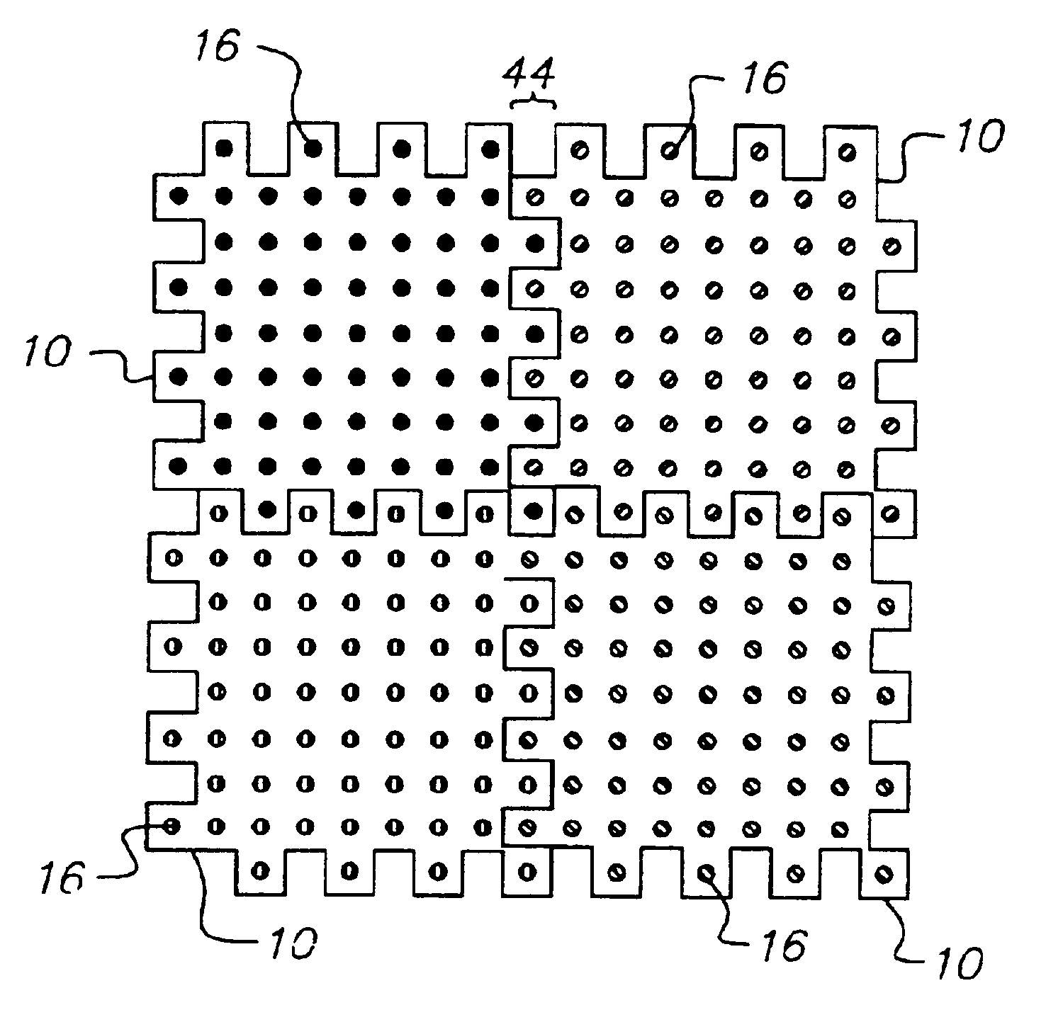
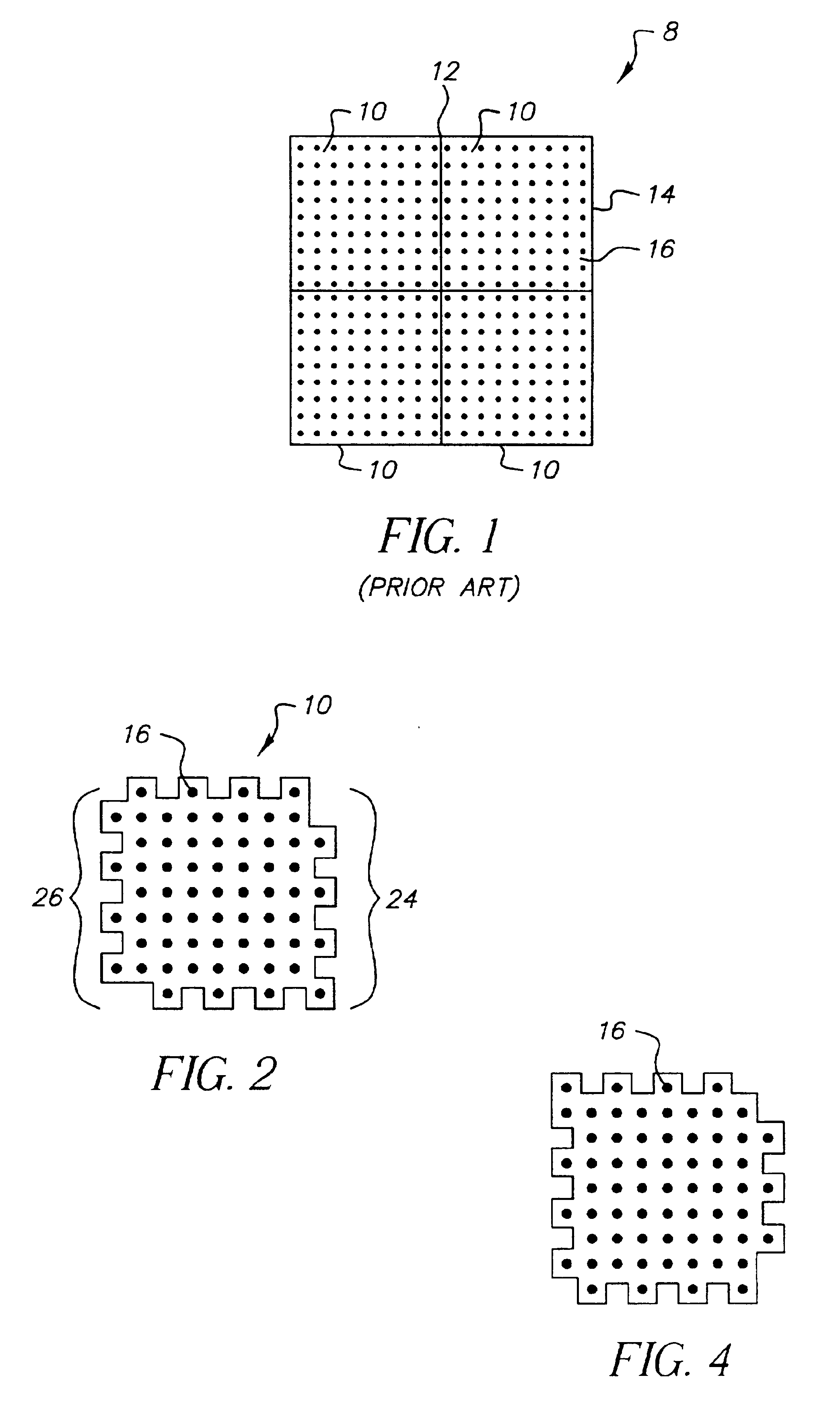
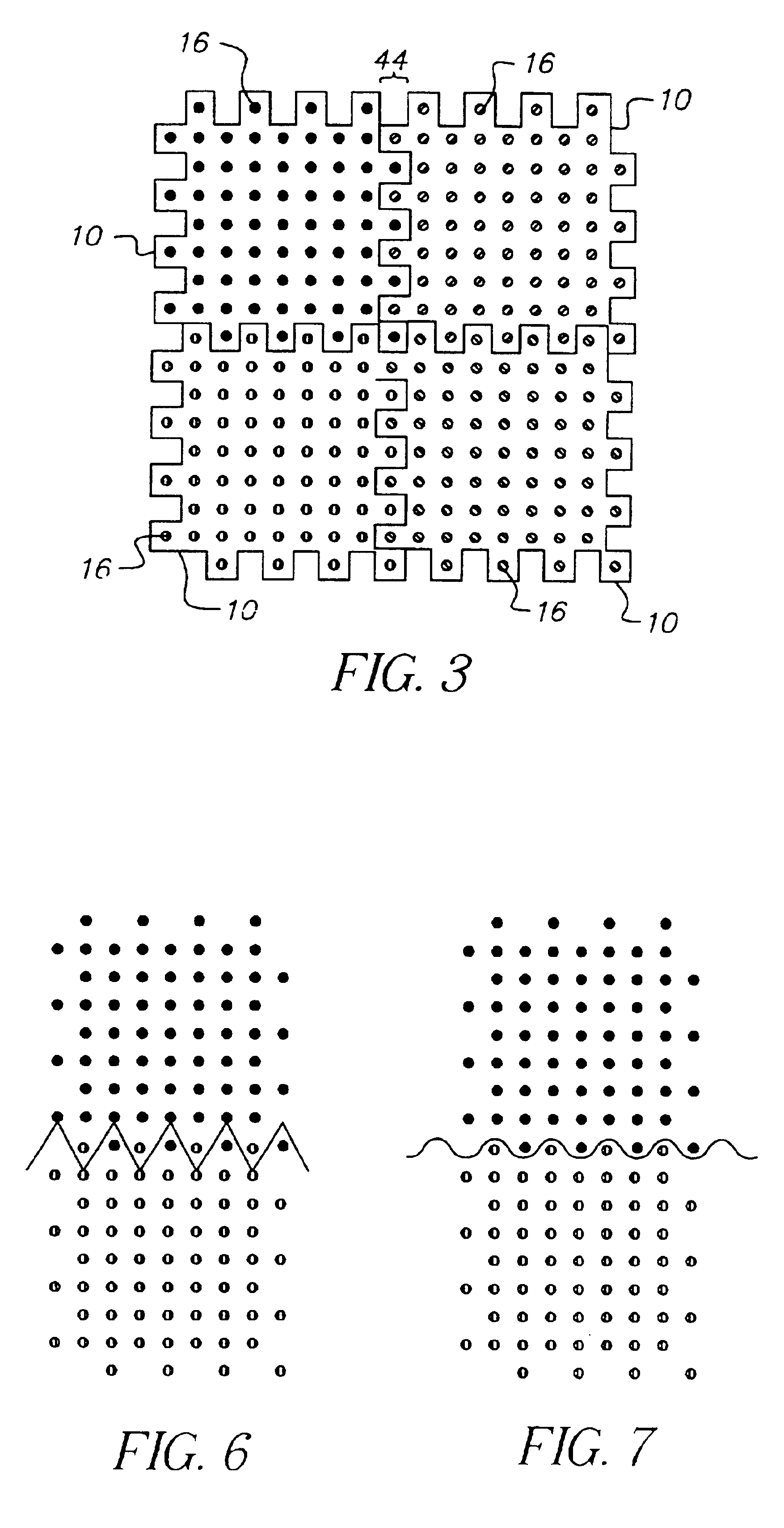
[0023]Referring to FIG. 1, a prior art tiled electro-optic imaging device (display or image sensor) 8 includes a two-by-two array of tiles 10, having edges 14 and an array of pixels 16. The edges 14 of the tiles 10 are aligned to produce a seam 12 between the edges of the tiles 14 and the last row or column of pixels 16 in the arrays. (The illustration of FIG. 1 is not drawn to scale to clarify the description). The edge seam 12 can be very visible to the human eye because it is straight, is horizontal or vertical, and has a direction that is the same as the pixel rows and columns. Moreover, small differences between the tiles, for example color, brightness, sensitivity or noise can be very visible to the human eye. According to the present invention, the perceived performance of the imaging device is improved by making the tile edges non-linear such that pixels from adjacent tiles are inter-digitated along the non-linear edge, whereby the visibility of the non-linear edge is reduce...


PUM

PropertyMeasurementUnit
sizeaaaaaaaaaa
coloraaaaaaaaaa
brightnessaaaaaaaaaa

Abstract

A tiled electro-optic imaging device includes two or more tiles each tile having a two dimensional array of pixels and at least one non-linear edge, the tiles being aligned edge to edge such that pixels from the tiles are inter-digitated along the non-linear edge, whereby the visibility of the non-linear edge is reduced and the visual uniformity of the device is enhanced.

Description

FIELD OF THE INVENTION[0001]The present invention relates to tiled electro-optic imaging devices such as displays and image sensors and, more particularly, to improving the visual appearance of such devices.BACKGROUND OF THE INVENTION[0002]It is known to increase the size of an electro-optic imaging device such as a flat panel display or an image sensor by forming the device using a plurality of tiles, each tile having a two dimensional array of pixels; see for example U.S. Pat. No. 6,262,696 issued Jul. 17, 2001 to Seraphim et al. Large tiled displays can also be made using an array of fiber optic panels in association with smaller displays. The fiber optic panels reduce the edge gap between the display tiles as described in U.S. Pat. No. 4,299,447 issued Nov. 10, 1981 to Soltan et al. WO 99 / 41732, Matthies et al., published Aug. 19, 1999, describes forming a tiled display device from display tiles having pixel positions defined up to the edge of the tiles. One example of the use o...

Claims


Application Information

Patent Timeline
Patent Type & Authority Patents(United States)
IPC IPC(8): G02B6/06G02B6/08H01L27/32H01L27/28H04N3/15H04N5/70G02F1/13G02F1/1333G09G3/32H05B33/10G09F9/40H01L27/14H01L27/146H01L51/50H04N5/335
CPCG02B6/06G02B6/08G02F1/133524G09G3/3208G09F9/3026H01L27/14603H01L27/3293H04N3/1593H04N5/70G02F1/13336G09G2300/026H04N25/41H10K59/18
Inventor COK, RONALD S.MILLER, MICHAEL E.
Owner GLOBAL OLED TECH
Why Eureka
Try Eureka