Liquid Crystal Display Device and Driving Method Thereof

a technology of liquid crystal display and driving method, which is applied in the field of liquid crystal display and the driving method thereof, can solve the problems of high cost and achieve the effects of reducing the number of leds, shortening the wait time, and increasing the time duration

Inactive Publication Date: 2012-12-20
TCL CHINA STAR OPTOELECTRONICS TECH CO LTD
View PDF4 Cites 3 Cited by
  • Summary
  • Abstract
  • Description
  • Claims
  • Application Information

AI Technical Summary

Benefits of technology

[0029]The present disclosure has the following benefits: as compared to the prior art, the LCD device and the driving method thereof of the present disclosure have a second TFT disposed in each pixel unit so that, after the pixel voltage is charged, the pixel voltage is stored into the first storage capacitor at first instead of being applied to the liquid crystal capacitor to tilt the liquid crystal molecules immediately. Meanwhile, the gates of the second TFTs are connected with each other. Then, after the gate of the last scan line is turned on and fully charged, the plurality of second TFTs are controlled to be turned on simultaneously so that the voltages across the first storage capacitors are introduced into the liquid crystal capacitors to tilt the liquid crystal molecules simultaneously, and the backlight can be turned on after the liquid crystal molecules tilt to a predetermined orientation. Because this shortens the time to wait for scanning of the gates and increases the time duration in which the backlight source emits light, the number of LEDs can be decreased to lower the cost. Meanwhile, because the backlight is provided across the whole surface but not section by section, the problems of nonuniform brightness and poor backlight coupling are overcome and the imaging quality is also improved.

Problems solved by technology

Because this shortens the time duration in which the backlight can be turned on, the number of LEDs must be increased to achieve a desired brightness level, thus leading to a higher cost.

Method used


Image

  • Liquid Crystal Display Device and Driving Method Thereof
  • Liquid Crystal Display Device and Driving Method Thereof
  • Liquid Crystal Display Device and Driving Method Thereof

Examples


Embodiment Construction

[0037]The present disclosure is more particularly described in the following examples that are intended as illustrative only since numerous modifications and variations therein will be apparent to those skilled in the prior art. Various embodiments of the disclosure are now described in detail. Referring to the drawings, like numbers indicate like parts throughout the views. As used in the description herein and throughout the claims that follow, the meaning of “a,”“an,” and “the” includes plural reference unless the context clearly dictates otherwise. Also, as used in the description herein and throughout the claims that follow, the meaning of “in” includes “in” and “on” unless the context clearly dictates otherwise.

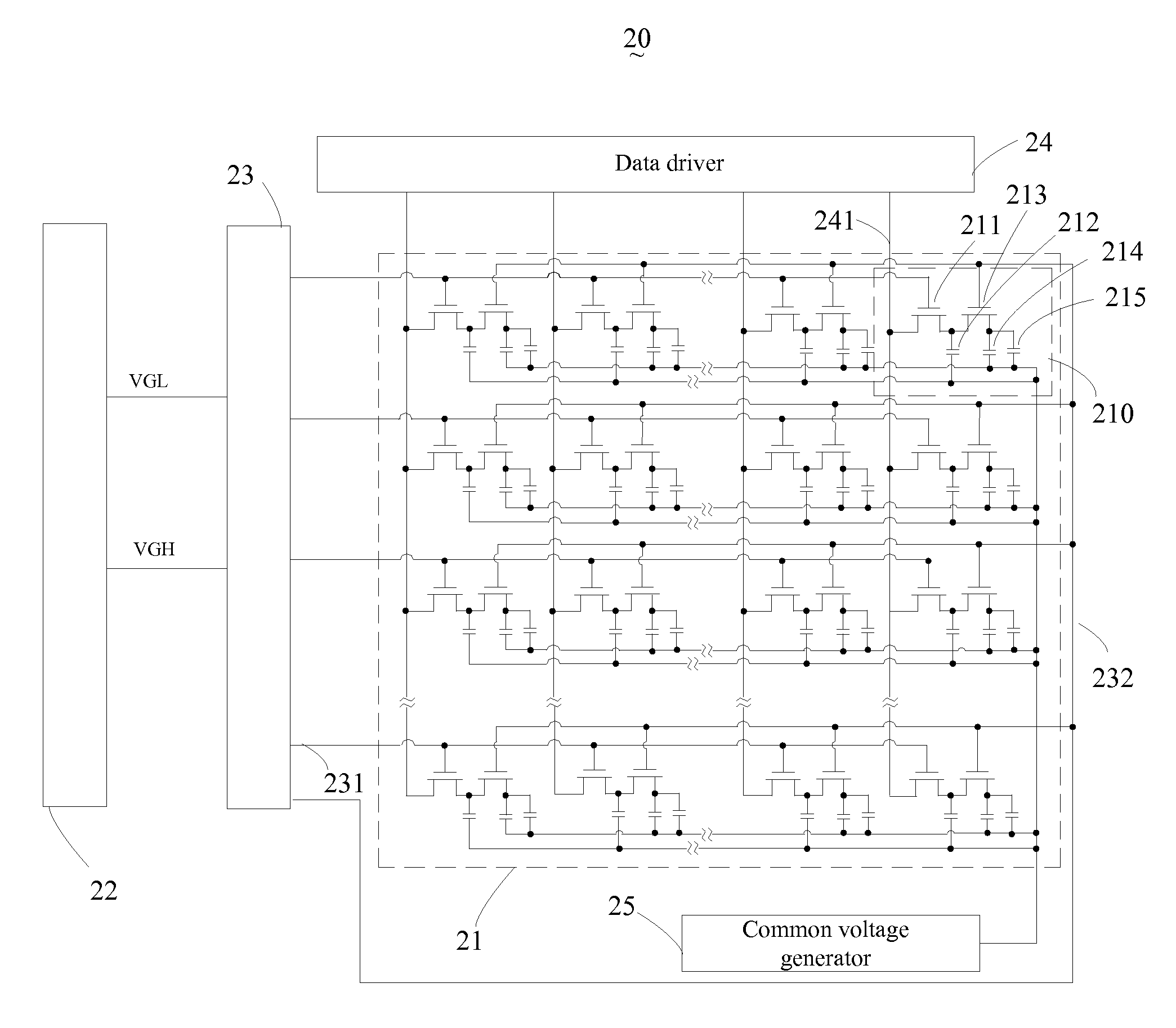
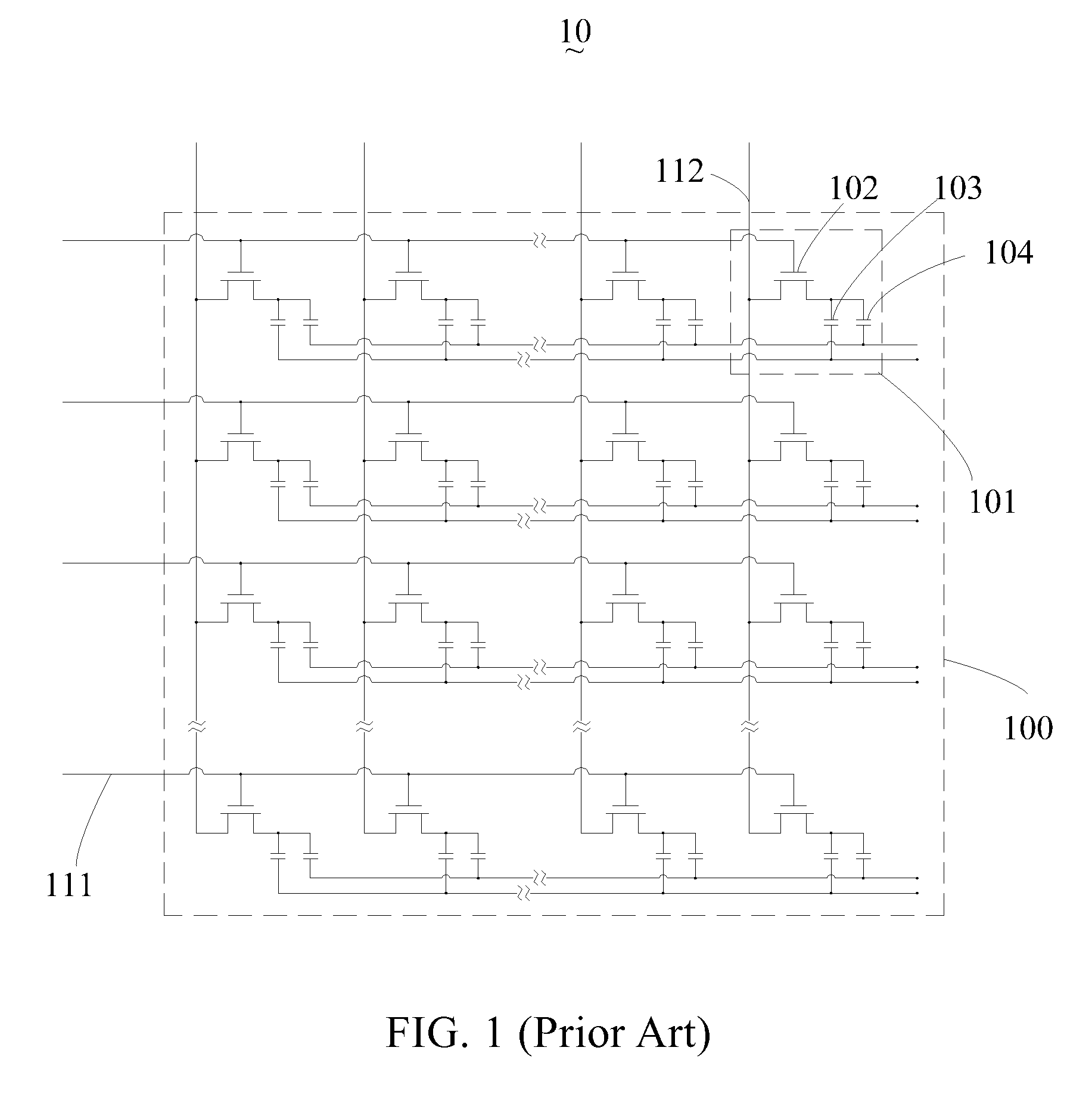
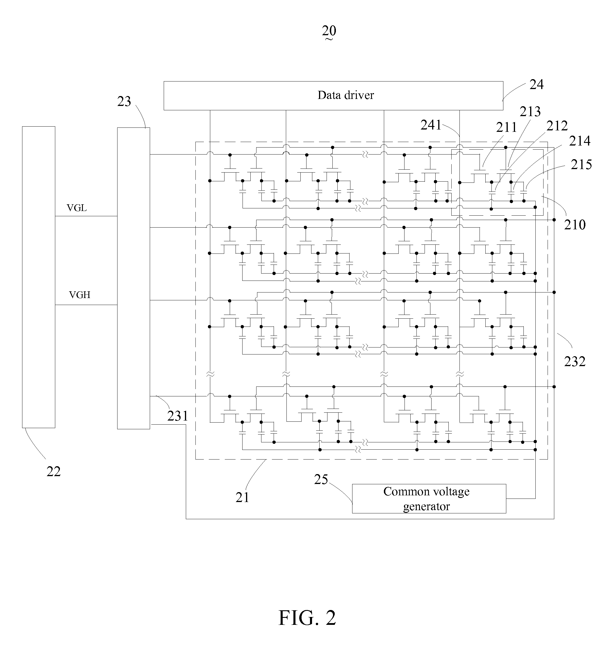
[0038]Referring to FIG. 2 and FIG. 3, FIG. 2 is a schematic circuit diagram of a preferred embodiment of an LCD device according to the present disclosure, and FIG. 3 is a schematic circuit diagram of each pixel unit shown in FIG. 2. As shown in FIG. 2, the LCD device 2...


PUM


Abstract

A liquid crystal display (LCD) device is disclosed. The LCD device comprises a plurality of pixel units arranged in the form of a matrix. Each of the pixel units comprises: a scan line; a data line; a first storage capacitor; a liquid crystal capacitor; and a first TFT, having a source electrically connected to the data line, a gate electrically connected to the scan line, and a drain electrically connected to the first storage capacitor. Each of the pixel units further comprises a second TFT, having a gate, a source electrically connected to the drain of the first TFT, and a drain electrically connected to the liquid crystal capacitor. The gates of the second TFTs are electrically connected with each other to control the second TFTs to be turned on simultaneously so as to tilt the liquid crystal molecules. Because this shortens the time to wait for scanning of the gates is shortened and increases the time duration in which the backlight can emit light, the number of LEDs can be reduced to lower the cost.

Description

FIELD OF THE INVENTION[0001]The present disclosure generally relates to the technical field of liquid crystal displaying, and more particularly, to a liquid crystal display (LCD) device and a driving method thereof.BACKGROUND OF THE INVENTION[0002]Nowadays, owing to such advantages as light weight, thin profile, low power consumption and low radiation, liquid crystal display (LCD) devices have found wide application in various electronic products such as computer monitors, TV sets, notebook computers, mobile phones, digital cameras and the like.[0003]Referring to FIG. 1, there is shown a schematic circuit diagram of an LCD device in the prior art. As shown in FIG. 1, the prior art LCD device 10 comprises a liquid crystal panel 100. The liquid crystal panel 100 comprises a plurality of scan lines 111 parallel with each other and a plurality of data lines 112 parallel with each other. The scan lines 111 and the data lines 112 intersect with and are insulated from each other to define ...

Claims


Application Information

Patent Timeline
Patent Type & Authority Applications(United States)
IPC IPC(8): G09G5/00G09G3/36
CPCG09G3/3659G09G3/3677G09G2300/0852G09G2310/0202G09G2320/0233G09G2320/0252
Inventor HOU, HUNG-LUNGHE, CHENGMING
Owner TCL CHINA STAR OPTOELECTRONICS TECH CO LTD
Why Eureka
Try Eureka