Flash memory device and manufacturing method thereof

Inactive Publication Date: 2012-11-08
INST OF MICROELECTRONICS CHINESE ACAD OF SCI
View PDF10 Cites 10 Cited by
  • Summary
  • Abstract
  • Description
  • Claims
  • Application Information

AI Technical Summary

Benefits of technology

[0007]The advantageous effect of the present invention is that the flash memory device comprises a polysilicon layer in the metal gate stack of the transistor area, which realizes the compatibility between the high-k dielectric metal gate and the erasable flash memory and makes it possible to apply the high-k dielectric metal gate into the one-time programmable (OTP) device so as to increase the operation performance of the flash memory.
[0009]The method of manufacturing the flash memory according to the present invention enables compatibility with the high-k dielectric metal gate process. Since the floating gate of the flash memory and the metal gate of the transistor adopt the same material and laminated structure, the same steps could be adopted in the methods of forming the flash memory and the transistor respectively on the same substrate. As a result, the process flow is greatly simplified and the production efficiency and homogeneity of products are increased, thereby providing favorable conditions for large-scale industrial production.

Problems solved by technology

Volatile memory devices will lose the stored data after interruption of the power supply, while non-volatile memory devices will still keep the stored data therein after interruption of the power supply.
However, while introducing the high-k dielectric metal gate process into the conventional process of making flash memories using complementary metal-oxide semiconductor (CMOS), the flash memory is greatly influenced in its erasability and cannot be repeatedly read and written for many times because data stored in the metal gate formed in the high-k dielectric metal gate process will not be easily erased by electric current.
As a result, there is a big challenge when applying the high-k dielectric metal gate process to the process of manufacturing of a one-time programmable (OTP) device.

Method used


Image

  • Flash memory device and manufacturing method thereof
  • Flash memory device and manufacturing method thereof
  • Flash memory device and manufacturing method thereof

Examples


Embodiment Construction

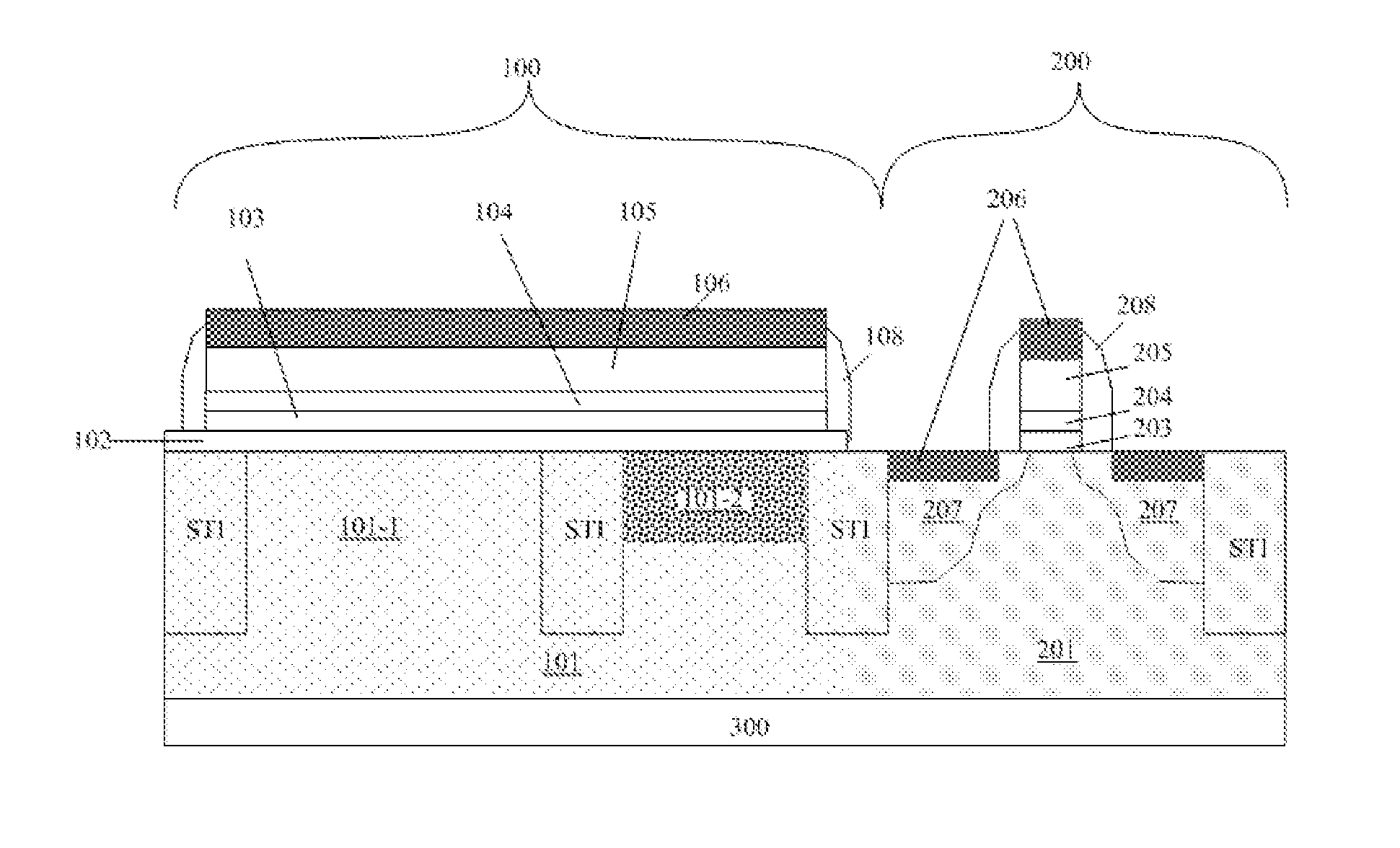
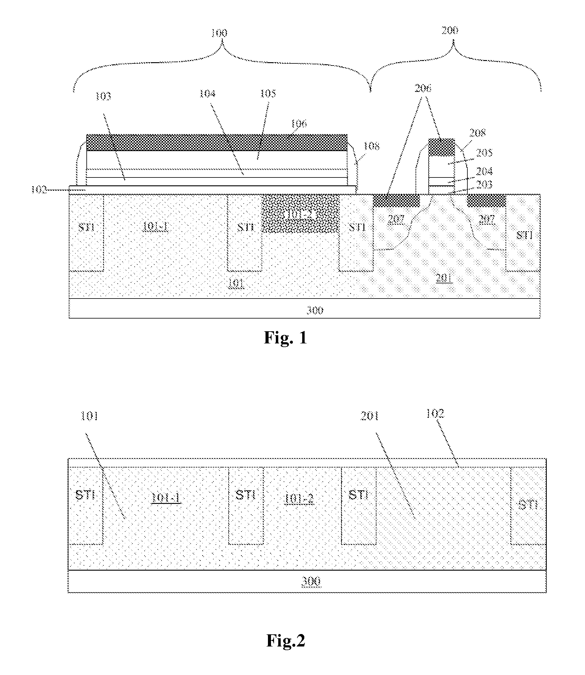
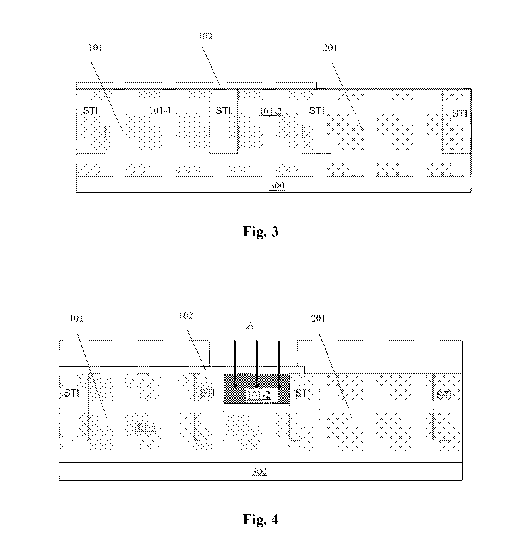
[0013]The embodiments of the present invention will be described in detail below, examples of which are shown in the drawings. The same or similar reference number indicates the same or similar element or the element having the same or similar function throughout the drawings. The embodiments described below with reference to the drawings are exemplary, and they are only for the purpose of illustrating the present invention rather than limiting the present invention.

[0014]The flash memory device of the present invention uses a metal gate electrode layer in the transistor area, which can not only overcome the defect of poor electrical erasability of the metal gate manufactured according to the high-k dielectric metal gate process, but also uniform the manufacturing processes of the flash memory and the transistor. Thus the manufacturing steps are simplified and the production efficiency is increased, and the flash memory made by the high-k dielectric metal gate process can be applied...


PUM


Abstract

The present invention discloses a flash memory device. The flash memory device comprises a semiconductor substrate and a flash memory area located on the semiconductor substrate. The flash memory area comprises a first doped well, which is divided into a first region and a second region by an isolation region, the second region being doped with an impurity having an electrical conductivity opposite to that of the first doped well; a high-k gate dielectric layer located on the first doped well; and a metal layer located on the high-k gate dielectric layer. The present invention enables compatibility between the high-k dielectric metal gate and the erasable flash memory and increases the operation performance of the flash memory. The present invention also provides a manufacturing method of the flash memory device, which greatly increases the production efficiency and yield of flash memory devices.

Description

FIELD OF THE INVENTION[0001]The present invention relates to the technical field of semiconductor manufacturing, in particular to a flash memory device and a manufacturing method thereof.DESCRIPTION OF THE PRIOR ART[0002]With the rapid development of computer technology, higher requirements are set forth to the performance of semiconductor memory devices. Semiconductor memory devices for storing data can be classified into two categories, i.e. volatile memory devices and non-volatile memory devices. Volatile memory devices will lose the stored data after interruption of the power supply, while non-volatile memory devices will still keep the stored data therein after interruption of the power supply. A flash memory is a non-volatile storage integrated circuit developed from erasable and programmable read-only memory (EPROM) and electrically erasable and programmable read-only memory (EEPROM). The flash memory is a one-time programmable (OTP) device having such main advantages as fast...

Claims


Application Information

Patent Timeline
IPC IPC(8): H01L29/792H01L21/336
CPCH01L21/823456H01L21/82385H01L27/112H01L27/11206H01L27/11519H01L29/7881H01L27/11541H01L27/11543H01L27/11558H01L29/66825H01L27/11521H10B20/20H10B20/00H10B41/10H10B41/47H10B41/48H10B41/60H10B41/30
Inventor ZHU, HUILONGLUO, ZHIJIONGYIN, HAIZHOU
Owner INST OF MICROELECTRONICS CHINESE ACAD OF SCI
Why Eureka
Try Eureka