
Planar Multiferroic/Magnetostrictive Nanostructures as Memory Elements, Two-Stage Logic Gates and Four-State Logic Elements for Information Processing

a multi-ferroic/magnetostrictive nanostructure and information processing technology, applied in semiconductor devices, digital storage, instruments, etc., can solve the problems of excessive energy (or heat) dissipation in the device, continued downscaling of digital electronic devices, and high energy consumption of current memory and logic circuits, so as to achieve energy efficiency and energy always a premium

Inactive Publication Date: 2012-10-25
VIRGINIA COMMONWEALTH UNIV
View PDF5 Cites 41 Cited by
  • Summary
  • Abstract
  • Description
  • Claims
  • Application Information

AI Technical Summary

Benefits of technology

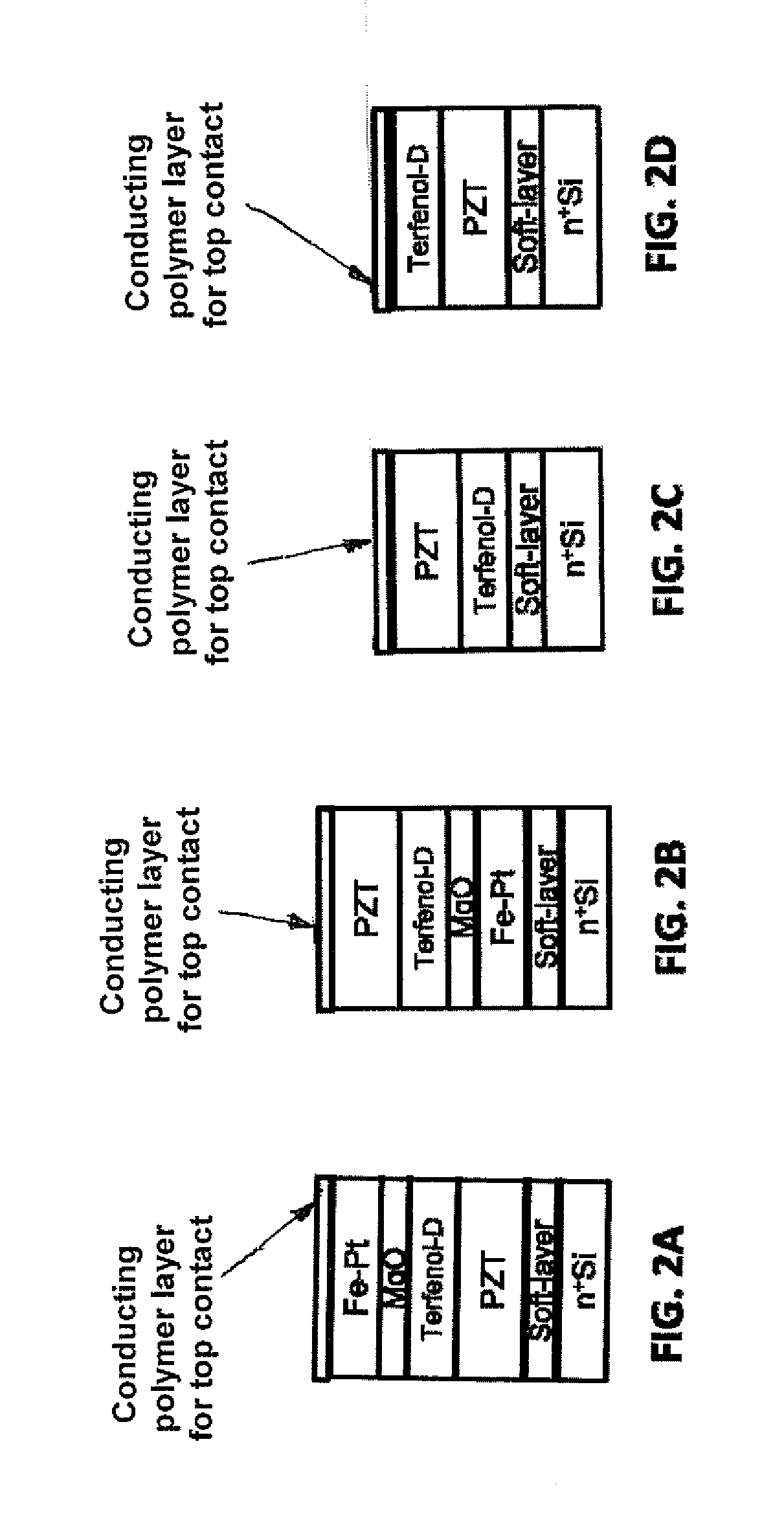
[0006]The device according to the invention consists of a magnetostrictive layer deposited over or under a piezoelectric layer or vice versa. Such a two-layer structure is called a multiferroic. The device is shaped like an elliptical cylinder so that the magnetization of the magnetostrictive layer can have only two stable states along the major axis of the ellipse. These two states encode the binary bits 0 and 1. Thus, it already behaves like a memory element storing digital bit information. In order to change the bit information (i.e., write new data into the memory), a voltage is applied across the piezoelectric layer. That generates strain in that layer, which is transferred to the magnetostrictive layer via elastic coupling. The strain rotates the magnetization of the magnetostrictive layer, thereby switching the magnet from one magnetization state to another (or switching the bit from 0 to 1, or vice versa). This switching is sufficient to use the device as a writable memory element, or a logic element. Reading of the stored bit is accomplished by vertically integrating a magneto-tunneling junction (MTJ) underneath the device. The latter consists of a ˜1 nm thin MgO layer and a hard magnet layer (e.g., Fe—Pt) of arbitrary thickness magnetized in a fixed direction. Note that synthetic anti-ferromagnet layer (SAF) separated from the hard (Fe—Pt) layer by a Ru spacer layer is added to minimize the dipole moment of the hard layer on the magnetostrictive layer. Measurement of the vertical resistance of the MTJ can unambiguously determine the magnetization state of the magnetostrictive layer and hence the stored bit.

Problems solved by technology

The primary obstacle to continued downscaling of digital electronic devices in accordance with Moore's law is the excessive energy (or heat) dissipation that takes place in the device during switching.
Current memory and logic circuits are very dissipative because they are transistor-based.
Transistors use electron charge to encode information, which is inherently inefficient.
Unfortunately, this advantage of magnets cannot be exploited unless the method employed to switch magnets is made energy-efficient.
Unfortunately, this method of switching dissipates too much energy, and a more energy-saving approach is desirable.

Method used


Image

  • Planar Multiferroic/Magnetostrictive Nanostructures as Memory Elements, Two-Stage Logic Gates and Four-State Logic Elements for Information Processing
  • Planar Multiferroic/Magnetostrictive Nanostructures as Memory Elements, Two-Stage Logic Gates and Four-State Logic Elements for Information Processing
  • Planar Multiferroic/Magnetostrictive Nanostructures as Memory Elements, Two-Stage Logic Gates and Four-State Logic Elements for Information Processing

Examples


Embodiment Construction

[0027]A multiferroic structure consists of a piezoelectric layer (e.g., PZT) and a magnetostrictive layer (e.g., Nickel or Terfenol-D) as shown in FIG. 1. If the lateral dimensions are on the order of 100 nm and the magnetostrictive layer's thickness is approximately 10 nm, then the latter behaves like a single-domain nanomagnet. The elliptical shape of this single domain nanomagnet ensures that its magnetization can have only two stable orientations when no stress is applied on it: along the major axis of the ellipse, i.e., the +y and −y axis. These two magnetization states encode “0” and “1” states when the magnet is used to store binary bits. When an electric voltage is applied across the piezoelectric layer, it deforms and the resulting stress / strain is transferred to the magnetostrictive layer on top. The stress anisotropy in the magnetostrictive layer then causes its magnetization to rotate. For materials with positive magnetostriction (e.g., Terfenol-D), tensile stress favors...


PUM


Abstract

A magnetostrictive-piezoelectric multiferroic single- or multi-domain nanomagnet whose magnetization can be rotated through application of an electric field across the piezoelectric layer has a structure that can include either a shape-anisotropic mangnetostrictive nanomagnet with no magnetocrystalline anisotropy or a circular nanomagnet with biaxial magnetocrystalline anisotropy with dimensions of nominal diameter and thickness. This structure can be used to write and store binary bits encoded in the magnetization orientation, thereby functioning as a memory element, or perform both Boolean and non-Boolean computation, or be integrated with existing magnetic tunneling junction (MTJ) technology to perform a read operation by adding a barrier layer for the MTJ having a high coercivity to serve as the hard magnetic layer of the MTJ, and electrical contact layers of a soft material with small Young's modulus. Equivalently, mangnetostrictive nanomagnetic elements whose magnetization is rotated by strain transferred from the substrate that has acoustic waves propagating on the substrate can be used.

Description

BACKGROUND OF THE INVENTION[0001]1. Field of the Invention[0002]The present invention generally relates to an ultra-low power / energy paradigm for memory, computing and information processing using multiferroic / magnetostrictive nanomagnets and, more particularly, to the use of planar multiferroic / magnetostrictive nanostructures as memory elements, two-state logic gates for traditional logic and four-state logic gates for performing higher order information processing. The invention includes novel multiferroic / magnetostrictive nanostructures design of memory elements, logic gates and other information processing elements with these structures, and processes for fabricating the same. These structures when used in memory or logic technology can potentially reduce energy consumption 1,000 to 10,000 times compared to the current state of the art, thereby enabling unique applications.[0003]2. Background Description[0004]The primary obstacle to continued downscaling of digital electronic de...

Claims


Application Information

Patent Timeline
IPC IPC(8): H01L29/82H01L21/02
CPCG11C11/16H01L27/20G11C11/1675H10B61/00H10N50/10H10N39/00
Inventor ATULASIMHA, JAYASIMHABANDYOPADHYAY, SUPRIYO
Owner VIRGINIA COMMONWEALTH UNIV
Learn More