
Vertical memory cell for high-density memory

Active Publication Date: 2012-10-18
MICRON TECH INC
View PDF21 Cites 78 Cited by
  • Summary
  • Abstract
  • Description
  • Claims
  • Application Information

AI Technical Summary

Problems solved by technology

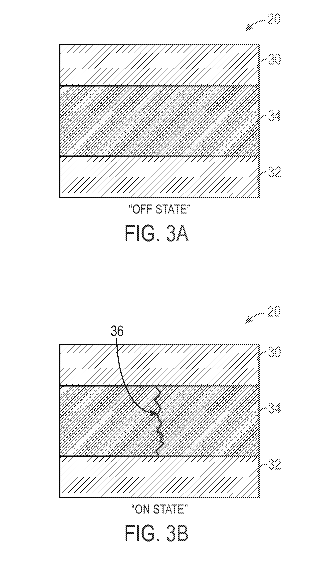
Removing the applied voltage or applying a different voltage (depending on the type of active material being used), may cause the conductive path to break or dispel, thus disconnecting the RRAM memory cell and returning it to the OFF state.
This may result in increasing cell-to-cell random variability due, for example, to continuum behavior breakdown and quantum effects that may become more apparent at such low dimensions.
Accordingly, control of the formation of conductive current pathways through variable resistance materials is often recognized as one of several challenging aspects in the design of resistive memory devices and, particularly, resistive memory devices at nanoscopic dimensions.

Method used


Image

  • Vertical memory cell for high-density memory
  • Vertical memory cell for high-density memory
  • Vertical memory cell for high-density memory

Examples


Embodiment Construction

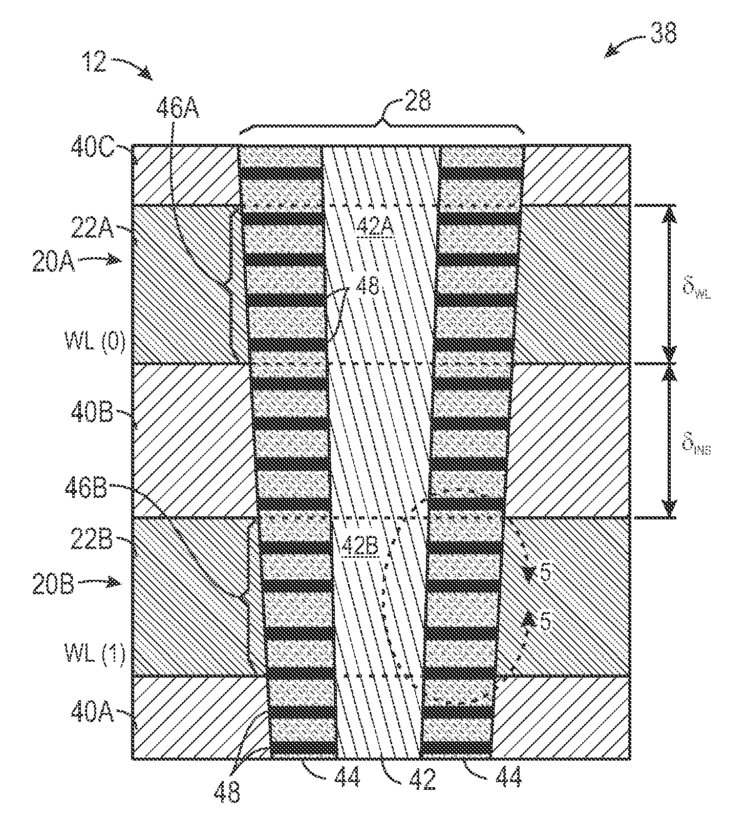
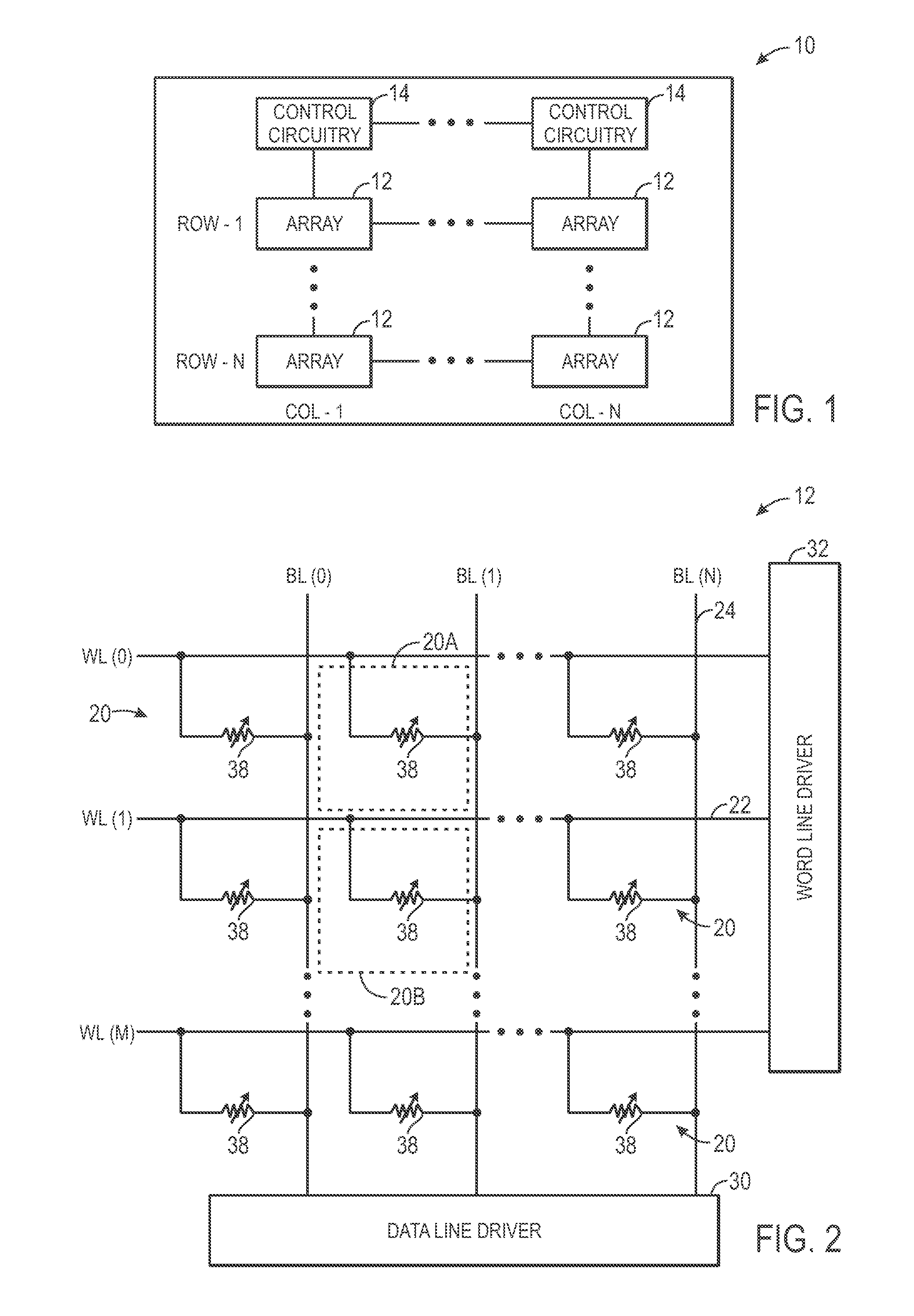
[0023]As discussed in further detail below, embodiments of the present invention relate to techniques for designing, manufacturing, and fabricating RRAM memory devices. In particular, certain embodiments provide vertical memory cell structures that may be implemented in RRAM devices. In one embodiment, cell area may be increased by word line height and / or interface surface characteristics to ensure the creation of a grain boundary that is suitable for formation of a preferential current path through an active layer of an RRAM memory cell. This may maintain continuum behavior while reducing random cell-to-cell variability that is often encountered at nanoscopic scales. By way of example, techniques relating to the formation of grain boundaries are disclosed in U.S. Pat. No. 7,883,929 (application Ser. No. 12 / 035,169), which is hereby incorporated by reference in its entirety. In another embodiment, the vertical memory cell structures may be formed in multiple-tiers to define a three-...


PUM


Abstract

This disclosure provides embodiments for the formation of vertical memory cell structures that may be implemented in RRAM devices. In one embodiment, memory cell area may be increased by varying word line height and / or word line interface surface characteristics to ensure the creation of a grain boundary that is suitable for formation of conductive pathways through an active layer of an RRAM memory cell. This may maintain continuum behavior while reducing random cell-to-cell variability that is often encountered at nanoscopic scales. In another embodiment, such vertical memory cell structures may be formed in multiple-tiers to define a three-dimensional RRAM memory array. Further embodiments also provide a spacer pitch-doubled RRAM memory array that integrates vertical memory cell structures.

Description

BACKGROUND[0001]1. Field of the Invention[0002]Embodiments of the present invention relate generally to the field of memory devices and, more particularly, to resistive random access memory (RRAM) devices.[0003]2. Description of the Related Art[0004]Electronic devices, such as computer systems, are often employed in numerous configurations to provide a variety of computing functions. For instance, computing speeds, system flexibility, applications, and form factor are typically some of the characteristics considered by design engineers tasked with the development of computing systems and their respective components. Often, such computing systems may include one or more memory devices which may be used to store applications (including program files and data) which may be accessible by other system components, such as one or more processors (e.g., CPU) or peripheral devices. By way of example, such memory devices may include volatile memory devices, such as dynamic random access memor...

Claims


Application Information

Patent Timeline
IPC IPC(8): H01L45/00
CPCH01L27/2463H01L27/249H01L45/06H01L45/08H01L45/085H01L45/147H01L45/142H01L45/143H01L45/144H01L45/146H01L45/1226H10B63/845H10B63/80H10N70/245H10N70/821H10N70/24H10N70/823H10N70/231H10N70/8822H10N70/8825H10N70/8836H10N70/8828H10N70/8833
Inventor SILLS, SCOTT E.SANDHU, GURTEJ
Owner MICRON TECH INC
Learn More