
Organic electroluminescent device

a technology of electroluminescent devices and electroluminescent devices, which is applied in the direction of luminescent compositions, thermoelectric devices, organic chemistry, etc., can solve the problems of inability to disclose the use of phosphorescent light-emitting devices as materials, failure to emit light at high efficiency, etc., to achieve secure the driving stability of the device, enhance the luminous efficiency of the device, and high luminous efficiency and driving stability

Active Publication Date: 2012-09-20
NIPPON STEEL CHEMICAL CO LTD
View PDF2 Cites 8 Cited by
  • Summary
  • Abstract
  • Description
  • Claims
  • Application Information

AI Technical Summary

Benefits of technology

[0016]In applications of organic EL devices to display devices such as flat panel displays, it is necessary to enhance the luminous efficiency of the device and, at the same time, to fully secure the driving stability of the device. Unde

Problems solved by technology

Europium complexes were also investigated in trials to utilize the excited triplet state, but they failed to emit light at high efficiency.
Since CBP is characterized by having a good hole transfer property but a poor electron transfer property, the use of CBP as a host material for tris(2-phenylpyridine)iridium complex (hereinafter referred to as Ir(ppy)3), a typical phosphorescent green light emitter, disturbs the balanced injection of charges and causes excessive holes to flow out to the side of the electron-transporting layer.
However, such use is demonstrated only in fluorescent light-emitting devices in the examples of the documents and it cannot be said that the use as materials for phosphorescent light-emitting devices is disclosed.

Method used


Image

  • Organic electroluminescent device
  • Organic electroluminescent device
  • Organic electroluminescent device

Examples


synthetic example 1

Synthesis of Compound 3-15

[0078]

[0079]Under a nitrogen atmosphere, 33.3 g (0.30 mol) of 1,2-cyclohexanedione, 86.0 g (0.60 mol) of phenylhydrazine hydrochloride, and 1,000 ml of ethanol were stirred at room temperature, 3.0 g (0.031 mol) of concentrated sulfuric acid was added dropwise over 5 minutes with stirring, and then the resulting solution was heated at 65° C. with stirring for 4 hours. The reaction solution was cooled to room temperature and the precipitated crystal was collected by filtration and washed with ethanol (2×500 ml) to give 80.0 g of a purplish brown crystal. This crystal, weighing 72.0 g (0.26 mol), was heated with 72.0 g of trifluoroacetic acid and 720.0 g of acetic acid at 100° C. with stirring for 15 hours. The reaction solution was cooled to room temperature and the precipitated crystal was collected by filtration, washed with acetic acid (200 ml), and purified by reslurrying to give 30.0 g (45% yield) of 5,12-dihydroindolo[2,3-a]carbazole (Compound IC-1) as...

example 1

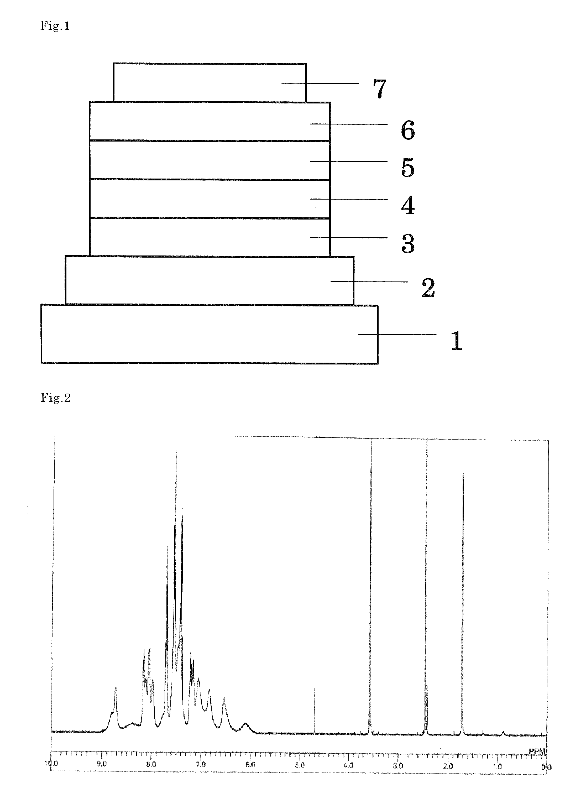
[0089]The constituent layers were deposited in thin film by the vacuum deposition process at a degree of vacuum of 4.0×10⁻⁵ Pa one upon another on a glass substrate on which a 110 nm-thick ITO anode had been formed. First, copper phthalocyanine (CuPc) was deposited on the ITO anode to a thickness of 25 nm. Then, 4,4′-bis[N-(1-naphthyl)-N-phenylamino]biphenyl (NPB) was deposited to a thickness of 40 nm as a hole-transporting layer. Next, Compound 3-15 obtained in Synthetic Example 1 as a host material and tris(2-phenylpyridine)iridium(III) (Ir(ppy)3) as a phosphorescend dopant were co-deposited from different deposition sources to a thickness of 40 nm as a light-emitting layer. The concentration of Ir(ppy)3 in the light-emitting layer was 10.0 wt %. Next, tris(8-hydroxyquinolinolato)aluminum(III) (Alq3) was deposited to a thickness of 20 nm as an electron-transporting layer. Then, lithium fluoride (LiF) was deposited on the electron-transporting layer to a thickness of 1.0 nm as an e...

example 2

[0091]An organic EL device was fabricated as in Example 1 except that Compound 1-31 was used as the host material in the light-emitting layer.


PUM


Abstract

Disclosed is an organic electroluminescent device (organic EL device) which is improved in luminous efficiency, sufficiently secures driving stability, and has a simple configuration. The organic EL device of this invention comprises a light-emitting layer between an anode and a cathode piled one upon another on a substrate and the light-emitting layer contains a phosphorescent dopant and an unsymmetrical indolocarbazole compound as a host material. The unsymmetrical indolocarbazole compound has a structure in which two or more groups having an indolocarbazole structure are linked together by a linking group and at least one of the groups has an isomeric indolocarbazole skeleton different from those of the other groups. Examples of the unsymmetrical indolocarbazole compound include compounds represented by the following formula (2) wherein A is a substituent, each of R1 to R3 is a hydrogen atom or a substituent, and L is a linking group composed of an aromatic group.

Description

TECHNICAL FIELD[0001]This invention relates to an organic electroluminescent device containing an indolocarbazole compound and, more particularly, to a thin film type device which emits light upon application of an electric field to a light-emitting layer composed of an organic compound.BACKGROUND TECHNOLOGY[0002]An organic electroluminescent device (hereinafter referred to as organic EL device) in the simplest structure is generally constituted of a light-emitting layer and a pair of counter electrodes holding the light-emitting layer between them. The organic EL device functions by utilizing the following phenomenon; upon application of an electric field between the electrodes, electrons are injected from the cathode and holes are injected from the anode and they recombine in the light-emitting layer with emission of light.[0003]In recent years, organic thin films have been utilized in the development of organic EL devices. In particular, in order to enhance the luminous efficienc...

Claims


Application Information

Patent Timeline
IPC IPC(8): H01L51/54
CPCC07D487/04C09K11/06C09K2211/1007C09K2211/1029C09K2211/1044H05B33/14C09K2211/1088H01L51/0072H01L51/0085H01L51/5016C09K2211/1074H10K85/6572H10K85/342H10K50/11H10K2101/10
Inventor KAI, TAKAHIROYAMAMOTO, TOSHIHIROKOMORI, MASAKIMATSUMOTO, MEGUMI
Owner NIPPON STEEL CHEMICAL CO LTD
Learn More