Static random access memory cell and method of operating the same
- Summary
- Abstract
- Description
- Claims
- Application Information
AI Technical Summary
Benefits of technology
Problems solved by technology
Method used
Image
Examples
embodiment 1
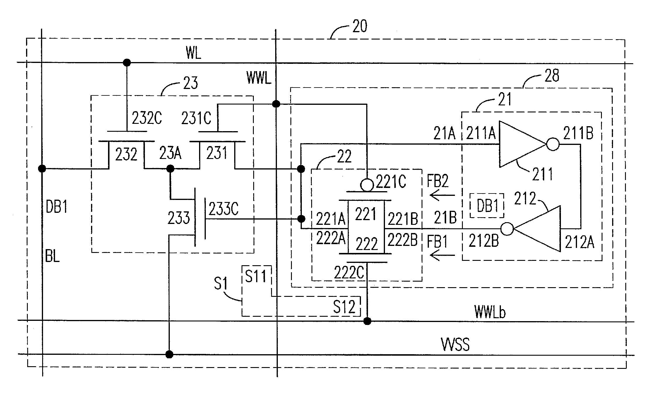
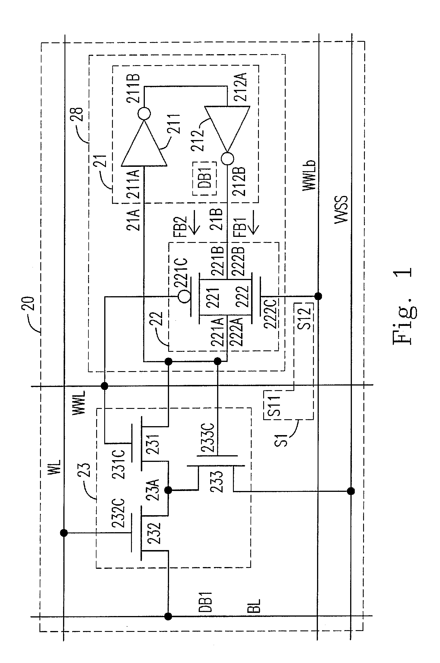
[0053]2. The SRAM cell is a subthreshold circuit, includes a single read / write port, and utilizes a reverse short channel effect.
[0054]3. The SRAM cell according to one of embodiments 1-2, wherein the bi-inverting circuit includes a first inverter and a second inverter. The first inverter has a first input terminal and a first storage node. The second inverter has a second storage node and a second input terminal electrically connected to the first storage node, wherein the feedback is a positive feedback, the first terminal is the first input terminal, and the second terminal is the second storage node.
[0055]4. The SRAM cell according to one of embodiments 1-3, wherein the switching circuit includes a first pass transistor and a second pass transistor. The first pass transistor is connected with the bi-inverting circuit in parallel, and has a first control terminal and a p-type conductivity. The second pass transistor is connected with the first pass transistor in parallel, and ha...
embodiment 10
[0062]11. The method , wherein the SRAM cell is a subthreshold circuit, and has a single read / write port.
[0063]12. The method according to one of embodiment 10-11, wherein wherein the SRAM cell further includes a latch unit including the bi-inverting circuit and the switching circuit, and the bi-inverting circuit includes a first inverter and a second inverter. The first inverter has a first input terminal and a first storage node. The second inverter has a second storage node and a second input terminal electrically connected to the first storage node, wherein the feedback is a positive feedback, the first terminal is the first input terminal, and the second terminal is the second storage node.
[0064]13. The method according to one of embodiment 10-12, wherein the switching circuit includes a first pass transistor and a second pass transistor. The first pass transistor is connected with the bi-inverting circuit in parallel, and has a first control terminal and a p-type conductivity....
embodiment 17
[0069]18. The SRAM cell according to the embodiment 17 further includes a latch unit including the bi-inverting circuit and the switching circuit, wherein the first connection state is a turn-off state, and the second connection state is a turn-on state; when the first connection state is formed, the SRAM cell loads a first data bit into the bi-inverting circuit; and when the second connection state is formed, a feedback is formed between the first terminal and the second terminal for holding the first data bit in the bi-inverting circuit.
[0070]19. The SRAM cell according to one of embodiments 17-18, wherein the first connection state is a turn-on state, and the second connection state is a turn-off state.
[0071]20. The SRAM cell according to one of embodiments 17-19, wherein when the first connection state is formed, a feedback is formed between the first terminal and the second terminal and the bi-inverting circuit is latched through the feedback; and when the second connection sta...
PUM
 Abstract
Description
Claims
Application Information
 - R&D
- Intellectual Property
- Life Sciences
- Materials
- Tech Scout
- Unparalleled Data Quality
- Higher Quality Content
- 60% Fewer Hallucinations
Browse by: Latest US Patents, China's latest patents, Technical Efficacy Thesaurus, Application Domain, Technology Topic, Popular Technical Reports.
© 2025 PatSnap. All rights reserved.Legal|Privacy policy|Modern Slavery Act Transparency Statement|Sitemap|About US| Contact US: help@patsnap.com


