Semiconductor light-emitting device and manufacturing method

a technology of semiconductors and light-emitting devices, which is applied in the manufacturing of semiconductor/solid-state devices, semiconductor devices, and semiconductor devices. it can solve the problems of difficult to provide wavelength-converted light having a high light-emitting efficiency and high light-emitting density, and the light-emitting device b>20/b>a may also be difficult to provide light with a high light-emitting efficiency and high light-emitting density, and achieve small-

Active Publication Date: 2012-08-23
STANLEY ELECTRIC CO LTD
View PDF7 Cites 49 Cited by
  • Summary
  • Abstract
  • Description
  • Claims
  • Application Information

AI Technical Summary

Benefits of technology

[0031]According to the exemplary manufacturing method described above for the semiconductor light-emitting devices, the inclined surface of the reflective material layer used as the focusing reflector can be formed by disposing an uncured reflective material between the frame and the side surfaces of the wavelength converting layer, the light-emitting chip and the optical plate. The wavelength converting layer and the reflective material layer can be solidified by a similar method as compared to conventional processes. Thus, the method can provide semiconductor light-emitting devices having a high light-emitting density and efficiency and a small light-emitting surface using manufacturing machines that are similar to those used to manufacture conventional semiconductor light-emitting devices.

Problems solved by technology

Thus, in the conventional light-emitting device 20 it may be difficult to provide a wavelength-converted light having a high light-emitting efficiency and a high light-emitting density from the small light-emitting surface 24 via the wavelength converting layer 21.
In addition, a circular bottom surface of the transparent dome 41 may be difficult to completely cover the top surface of the substrate 25 formed in a square shape therewith, and therefore may be difficult to receive light emitted from a square light-emitting surface including four corners of the light-emitting region 28 at high efficiency.
Thus, the conventional light-emitting device 20A may also be difficult to provide light having a high light-emitting efficiency and a high light-emitting density from the small light-emitting surface, even though the device 20A may form various small light-emitting surfaces.
Thus, the conventional light-emitting device 50 may also be difficult to provide a wavelength-converted light having a high light-emitting efficiency and a high light-emitting density from the small light-emitting surface, although the device 50 may improve a contrast between the light-emitting portion and the non-light-emitting portion.

Method used


Image

  • Semiconductor light-emitting device and manufacturing method
  • Semiconductor light-emitting device and manufacturing method
  • Semiconductor light-emitting device and manufacturing method

Examples


first embodiment

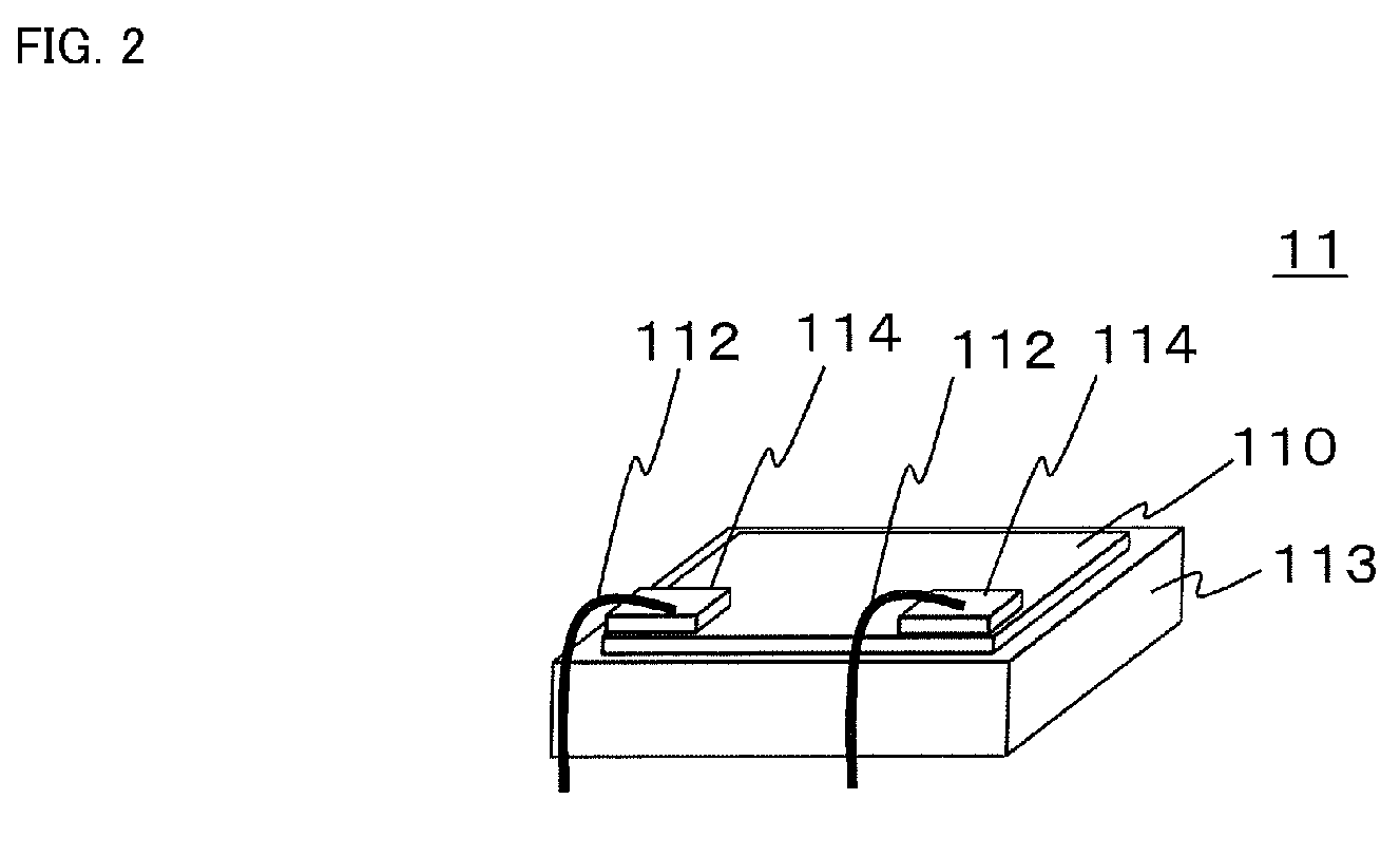
[0060]FIG. 2 is a perspective view depicting the exemplary semiconductor light-emitting chip 11 used in the semiconductor light-emitting device shown in FIG. 1. The light-emitting chip 11 can include the substrate 113, and the semiconductor layer 110 located on the substrate 113 as described above. The semiconductor layer 110 can include a plurality of epitaxially grown semiconductor layers, and also can include the light-emitting layer, which emits light having an emission wavelength by supply a driving current between a pair of top electrodes 114.

[0061]The substrate 113 of the light-emitting chip 11 can be made of an opaque material such as silicon carbide, etc. When the silicon carbide is used as the substrate 113 of the light-emitting chip 11, one of the top electrodes 114 can also be located adjacent the bottom surface of the substrate 113 as a bottom electrode because the silicon carbide substrate is an electrical conductive material. In this case, the light-emitting chip 11 c...

third embodiment

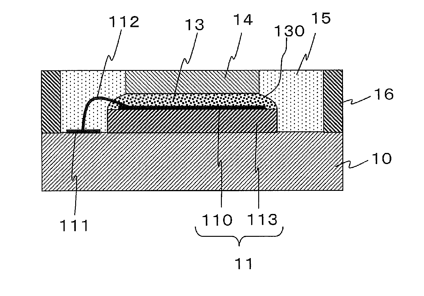
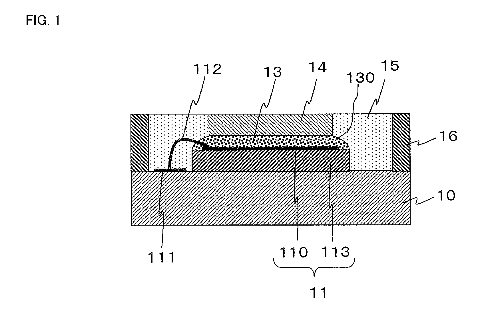
[0111]FIGS. 9a and 9b are a side cross-sectional view and a top view showing the semiconductor light-emitting device made in accordance with principles of the disclosed subject matter, respectively. The light-emitting device can include an optical plate 14 having an edge located between a side surface and a bottom surface thereof, being located over the top surface of each of the semiconductor layers 110 so that the bottom surface thereof can overlap the top surface of each of the semiconductor layers 110.

[0112]In addition, the light-emitting device can include a wavelength converting layer 13 disposed between the edge of the optical plate 14 and the edge of the semiconductor light-emitting chips so that a inclined surface 130 thereof extends from the edge of the optical plate 14 toward the edge of the semiconductor light-emitting chips 11, while also encapsulating the semiconductor layers 110 and parts of bonding wires 112.

[0113]Moreover, the device can include a frame 16 and a ref...


PUM


Abstract

A semiconductor light-emitting device and a method for manufacturing the same can include a wavelength converting layer located over at least one semiconductor light-emitting chip in order to emit various colored lights including white light. The light-emitting device can include a base board, a frame located on the base board, the chip mounted on the base board, the wavelength converting layer located between an optical plate and the chip so as to extend from the optical plate toward the chip, and a reflective material layer disposed at least between the frame and both side surfaces of the wavelength converting layer and the optical plate.

Description

[0001]This application claims the priority benefit under 35 U.S.C. §119 of Japanese Patent Application No. 2011-028841 filed on Feb. 14, 2011, which is hereby incorporated in its entirety by reference.BACKGROUND[0002]1. Field[0003]The presently disclosed subject matter relates to semiconductor light-emitting devices in which light emitted from a semiconductor light-emitting chip is wavelength-converted by a wavelength converting layer, and to manufacturing methods for the same. More particularly, the disclosed subject matter relates to semiconductor light-emitting devices for a vehicle light and the like, which can emit light having a high light-emitting density and efficiency from a small light-emitting surface, and to methods of manufacturing such devices.[0004]2. Description of the Related Art[0005]Semiconductor light-emitting devices, in which a part of the light emitted from a semiconductor light-emitting chip is converted into light having a different wavelength by a phosphor ...

Claims


Application Information

Patent Timeline
Patent Type & Authority Applications(United States)
IPC IPC(8): H01L33/08H01L33/60
CPCH01L33/501H01L33/56H01L2933/0041H01L2933/005H01L2224/8592H01L2224/48091H01L2924/00014
Inventor HARADA, MITSUNORI
Owner STANLEY ELECTRIC CO LTD
Why Eureka
Try Eureka