Coated article and method for making same
a technology of coated articles and coatings, applied in the field of coated articles, can solve the problem of limiting the application of organic hydrophobic materials to the next level
- Summary
- Abstract
- Description
- Claims
- Application Information
AI Technical Summary
Benefits of technology
Problems solved by technology
Method used
Image
Examples
example 1
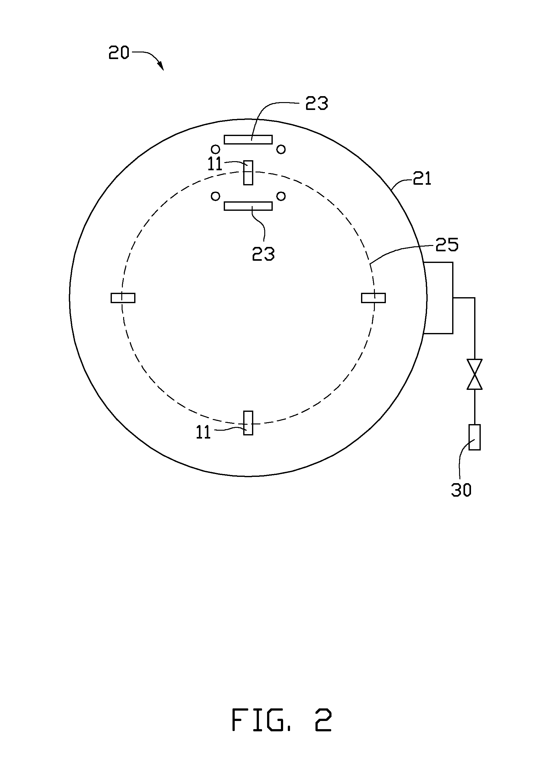
[0020]The vacuum sputtering device 20 used in example 1 was a medium frequency magnetron sputtering device (model No. SM-1100H) manufactured by South Innovative Vacuum Technology Co., Ltd., located in Shenzhen, China.
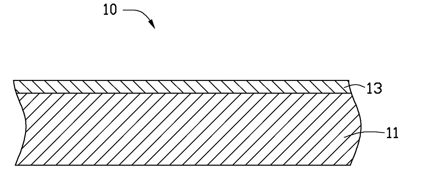
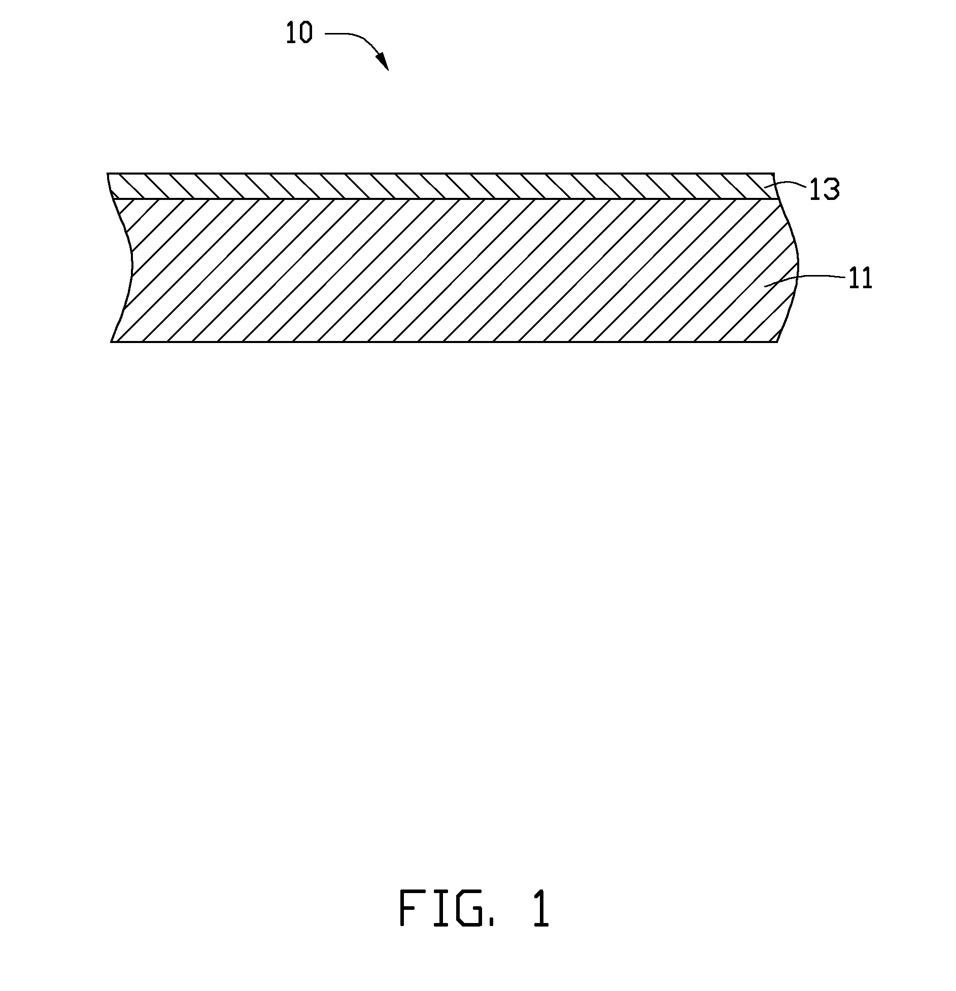
[0021]The substrate 11 was made of glass.
[0022]Plasma cleaning: Ar was fed into the vacuum chamber 21 at a flow rate of about 500 sccm. A negative bias voltage of about −100 V was applied to the substrate 11. The plasma cleaning of the substrate 11 took about 5 min.
[0023]Sputtering to form the hydrophobic layer 13: The vacuum chamber 21 was heated to about 200° C. Ar was fed into the vacuum chamber 21 at a flow rate of about 350 sccm. Ammonia gas was fed into the vacuum chamber 21 at a flow rate of about 200 sccm. The power of the graphite targets 23 was 8 kw and a negative bias voltage of −120 V was applied to the substrate 11. The depositing of the hydrophobic layer 13 took 40 min. The hydrophobic layer 13 had a thickness of about 200 nm.
example 2
[0024]The vacuum sputtering device 20 used in example 2 was the same in example 1.
[0025]The substrate 11 was made of stainless steel.
[0026]Plasma cleaning: Ar was fed into the vacuum chamber 21 at a flow rate of about 500 sccm. A negative bias voltage of about −150 V was applied to the substrate 11. Plasma cleaning of the substrate 11 took about 5 min.
[0027]Sputtering to form the hydrophobic layer 13: The vacuum chamber 21 was heated to about 200° C. Ar was fed into the vacuum chamber 21 at a flow rate of about 250 sccm. Ammonia gas was fed into the vacuum chamber 21 at a flow rate of about 245 sccm. The power of the graphite targets 23 was 10 kw and a negative bias voltage of about −200 V was applied to the substrate 11. The depositing of the hydrophobic layer 13 took 50 min. The hydrophobic layer 13 had a thickness of about 300 nm.
Results of the Above Examples
[0028]The water contact angles of the coated articles 10 made in example 1 and 2 were measured using a contact angle measur...
PUM
| Property | Measurement | Unit |
|---|---|---|
| Temperature | aaaaa | aaaaa |
| Temperature | aaaaa | aaaaa |
| Volumetric flow rate | aaaaa | aaaaa |
Abstract
Description
Claims
Application Information
 - R&D
- Intellectual Property
- Life Sciences
- Materials
- Tech Scout
- Unparalleled Data Quality
- Higher Quality Content
- 60% Fewer Hallucinations
Browse by: Latest US Patents, China's latest patents, Technical Efficacy Thesaurus, Application Domain, Technology Topic, Popular Technical Reports.
© 2025 PatSnap. All rights reserved.Legal|Privacy policy|Modern Slavery Act Transparency Statement|Sitemap|About US| Contact US: help@patsnap.com


