Silicon carbide substrate, semiconductor device, method of manufacturing silicon carbide substrate and method of manufacturing semiconductor device
semiconductor technology, applied in the direction of individual semiconductor device testing, semiconductor/solid-state device testing/measurement, instruments, etc., can solve the problem of large reverse leakage current, and achieve the effect of reducing the reverse leakage current in the semiconductor device having a silicon carbide substra
- Summary
- Abstract
- Description
- Claims
- Application Information
AI Technical Summary
Benefits of technology
Problems solved by technology
Method used
Image
Examples
embodiment 1
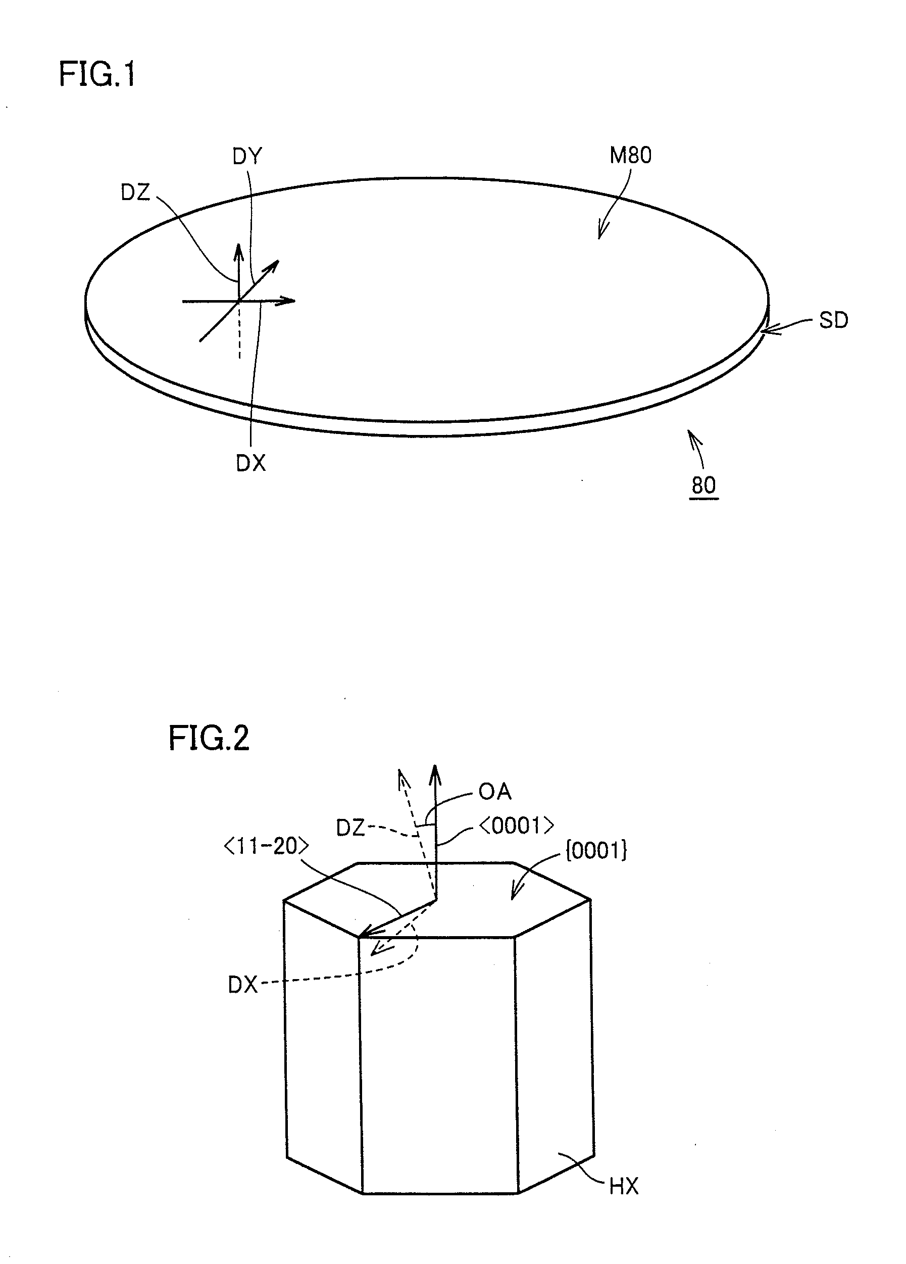
[0051]As shown in FIG. 1, a silicon carbide substrate in accordance with the present invention is a single crystal substrate 80 (silicon carbide substrate) formed of silicon carbide having hexagonal crystal structure. Single crystal substrate 80 has a side surface SD and a main surface M80 surrounded by the side surface SD. Polytype of the hexagonal crystal is, preferably, 4H.
[0052]Further, as shown in FIG. 2, main surface M80 (FIG. 1) is tilted by an off angle OA relative to {0001} plane of the hexagonal crystal HX. Specifically, normal direction DZ of main surface M80 is inclined by off angle OA from direction. The tilting is in off direction DX. In the figure, a direction DY represents a direction perpendicular to the direction DX. In the present embodiment, the off direction DX corresponds to direction on the {0001} plane.
[0053]Main surface M80 of single crystal substrate 80 has specific photoluminescence characteristics as will be described later. Measurement of photoluminesc...
embodiment 2
[0094]As shown in FIG. 13, the silicon carbide substrate in accordance with the present embodiment is an epitaxial substrate 90 (silicon carbide substrate) having a silicon carbide layer 81 with a main surface M90 and a single crystal substrate 80 (base substrate) supporting silicon carbide layer 81. Silicon carbide layer 81 is epitaxially formed on single crystal substrate 80.
[0095]Main surface M90 of epitaxial substrate 90 has specific photoluminescence characteristics as described later. A method of measuring photoluminescence characteristics will be described in the following.
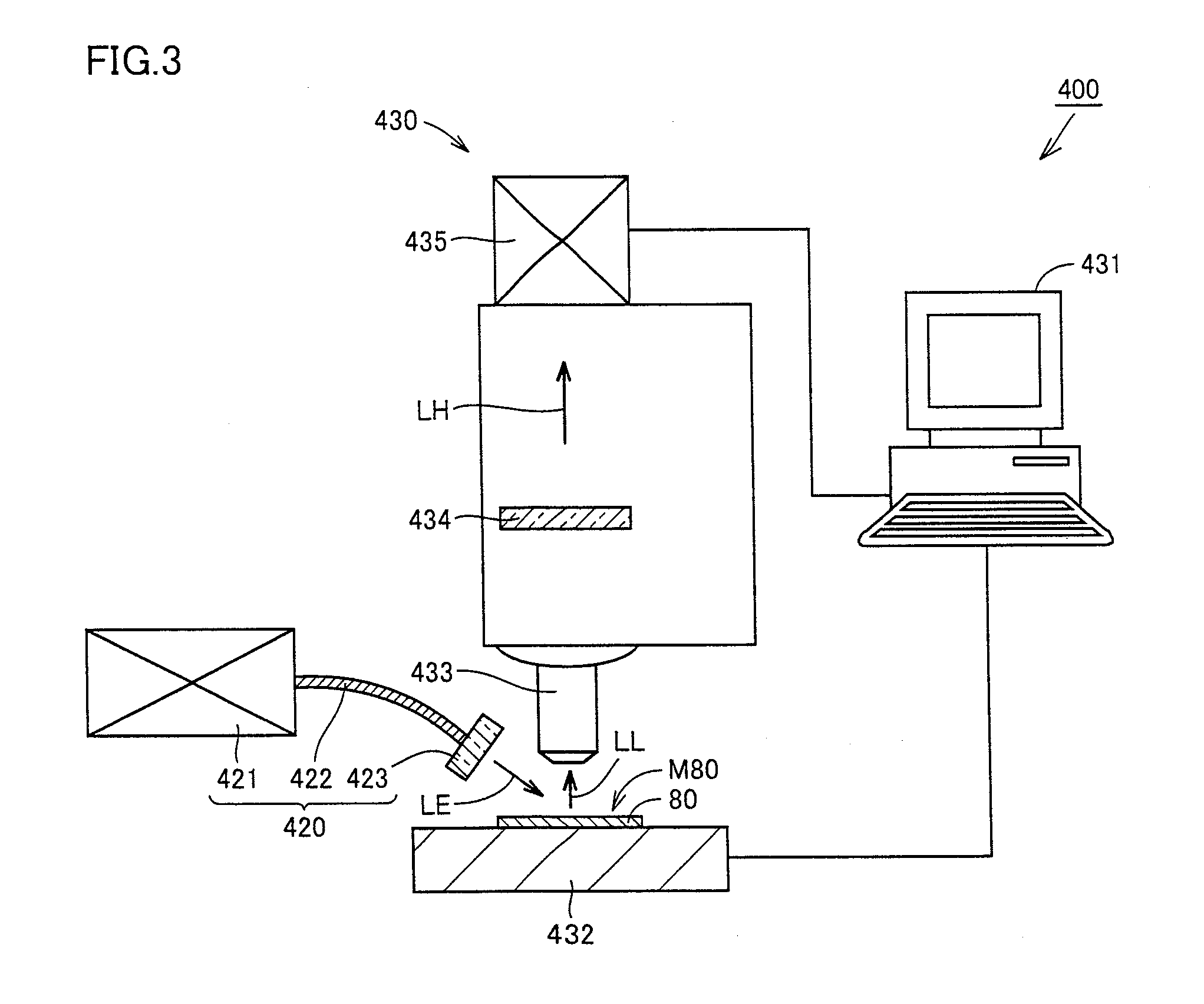
[0096]As shown in FIG. 14, epitaxial substrate 90 is mounted on a photoluminescence measuring apparatus 400. Main surface M90 of epitaxial substrate 90 is irradiated with excitation light LE. Consequently, emission of photoluminescent light LL occurs on main surface M90. Transmitted light LH, which is photoluminescent light LL passed through filter 434, is observed as an image by camera 435. Specifically, o...
embodiment 3
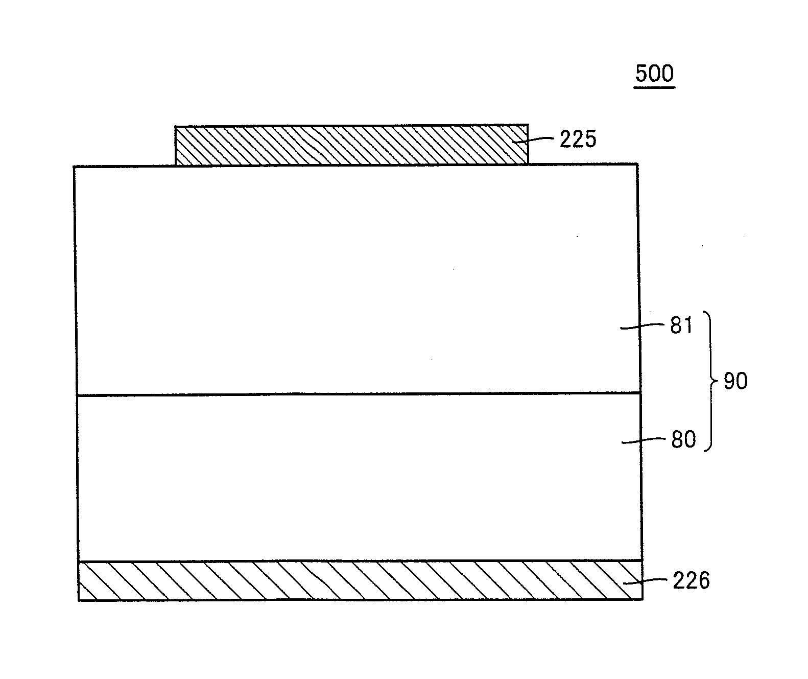
[0109]As shown in FIG. 18, a semiconductor device in accordance with the present embodiment is a Schottky diode 500 (semiconductor device) having epitaxial substrate 90. Schottky diode 500 has epitaxial substrate 90, an anode electrode 225 and a cathode electrode 226. Anode electrode 225 is provided on a main surface on the side of silicon carbide layer 81 of epitaxial substrate 90. The cathode electrode is provided on a surface on the side of single crystal substrate 80 of epitaxial substrate 90.
[0110]Single crystal substrate 80 has n+ conductivity type, and silicon carbide layer 81 has n− conductivity type. Thickness of single crystal substrate 80 is, for example, at least 300 μm and at most 400 μm. By way of example, single crystal substrate 80 contains nitrogen atoms as an impurity, of which concentration is about 1×1019 cm−3. The thickness of silicon carbide layer 81 is, for example, 10 μm. By way of example, silicon carbide layer 81 contains nitrogen atoms as an impurity, of w...
PUM
 Abstract
Description
Claims
Application Information
 - R&D
- Intellectual Property
- Life Sciences
- Materials
- Tech Scout
- Unparalleled Data Quality
- Higher Quality Content
- 60% Fewer Hallucinations
Browse by: Latest US Patents, China's latest patents, Technical Efficacy Thesaurus, Application Domain, Technology Topic, Popular Technical Reports.
© 2025 PatSnap. All rights reserved.Legal|Privacy policy|Modern Slavery Act Transparency Statement|Sitemap|About US| Contact US: help@patsnap.com


