Semiconductor package module

a technology of semiconductors and package modules, applied in the direction of cross-talk/noise/interference reduction, sustainable manufacturing/processing, final product manufacturing, etc., can solve the problems of difficult electrical connection of ground patterns formed on the upper surface of substrates to shields, damage to connection portions, etc., and achieve excellent electromagnetic interference (emi) and electromagnetic susceptibility characteristics

Inactive Publication Date: 2012-05-03
SAMSUNG ELECTRO MECHANICS CO LTD
View PDF7 Cites 23 Cited by
  • Summary
  • Abstract
  • Description
  • Claims
  • Application Information

AI Technical Summary

Benefits of technology

[0011]An aspect of the present invention provides a semiconductor package module including an electromagnetic shielding structure having excellent electromagnetic interference (EMI) and electromagnetic susceptibility (EMS) characteristics, while protecting individual elements therein from shocks.
[0012]Another aspect of the present invention provides a semiconductor package module capable of easily grounding a shield.
[0013]Another aspect of the present invention provides a semiconductor package module capable of securing bonding reliability between a shield and a ground pattern.

Problems solved by technology

Accordingly, it was difficult to electrically connect the ground pattern formed on an upper surface of the substrate to the shield.
In addition, according to the related art, since the ground pattern of the substrate was directly electrically connected to the shield, a connection portion therebetween was formed by a very fine pattern, whereby the connection portion was damaged due, to shocks, or the like.

Method used


Image

  • Semiconductor package module
  • Semiconductor package module
  • Semiconductor package module

Examples


Embodiment Construction

[0034]The terms and words used in the present specification and claims should not be interpreted as being limited to typical meanings or dictionary definitions, but should be interpreted as having meanings and concepts relevant to the technical scope of the present invention based on the rule according to which an inventor can appropriately define the concept of the term to describe most appropriately the best method he or she knows for carrying out the invention. Therefore, the configurations described in the embodiments and drawings of the present invention are merely the most preferable embodiments, but do not represent the overall technical spirit of the present invention. Thus, the present invention should be construed as including all of the changes, equivalents, and substitutions included in the spirit and scope of the present invention at the time of filing this application.

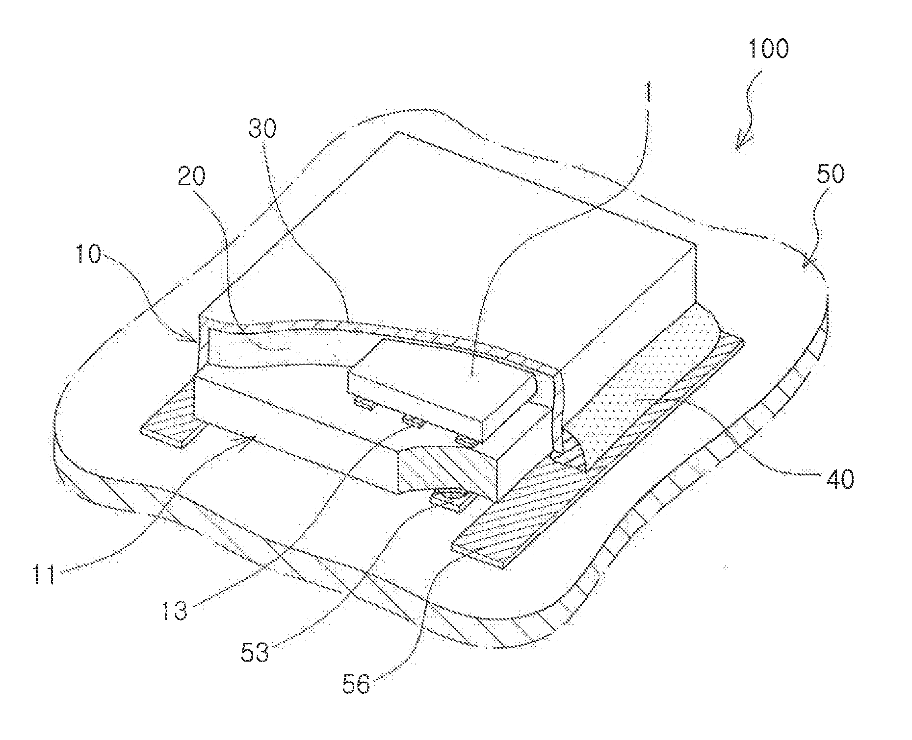
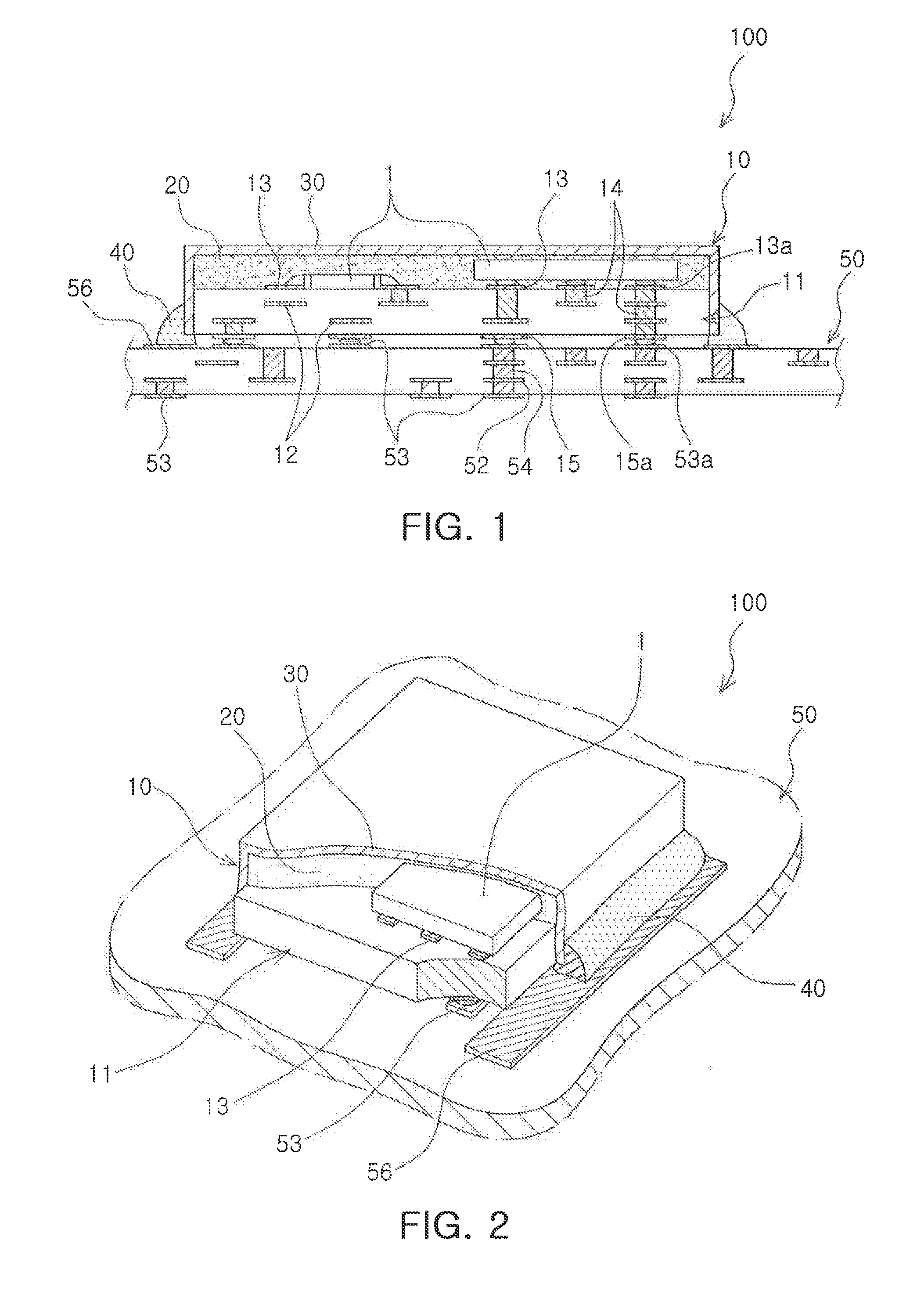
[0035]Hereinafter, exemplary embodiments of the present invention will be described in detail with ref...


PUM


Abstract

There is provided a semiconductor package module allowing a shield of a semiconductor package to be easily grounded and securing bonding reliability between the shield and a ground pattern. The semiconductor package module includes a semiconductor package having a shield formed on an upper surface thereof and side surfaces thereof; a main substrate having at least one ground electrode formed on a surface thereof and having the semiconductor package mounted thereon; and a bonding part bonding the ground electrode to the shield to electrically connect the ground electrode to the shield.

Description

CROSS-REFERENCE TO RELATED APPLICATIONS[0001]This application claims the priority of Korean Patent Application No. 10-2010-0107768 filed on Nov. 1, 2010, in the Korean Intellectual Property Office, the disclosure of which is incorporated herein by reference.BACKGROUND OF THE INVENTION[0002]1. Field of the Invention[0003]The present invention relates to a semiconductor package module, and more particularly, to a semiconductor package module including a shielding member capable of shielding electromagnetic waves while simultaneously protecting a passive element, a semiconductor chip, or the like, included in a package from an external environment.[0004]2. Description of the Related Art[0005]In accordance with a recent rapid increase in the demand for portable apparatuses in an electronic product market, the demand for compact, light-weight electronic components mounted within these products has continuously increasing.[0006]In order to manufacture compact, light-weight electronic comp...

Claims


Application Information

Patent Timeline
Patent Type & Authority Applications(United States)
IPC IPC(8): H01L23/552
CPCH01L23/3128H01L23/552H01L24/16H01L2224/16225H05K1/0216H05K1/111H05K2201/10371H01L2924/19105Y02P70/50
Inventor KIM, JUNG WOO
Owner SAMSUNG ELECTRO MECHANICS CO LTD
Why Eureka
Try Eureka