
Compact folded configuration for integrated circuit packaging

Inactive Publication Date: 2012-02-23
APPLE INC
View PDF3 Cites 13 Cited by
  • Summary
  • Abstract
  • Description
  • Claims
  • Application Information

AI Technical Summary

Benefits of technology

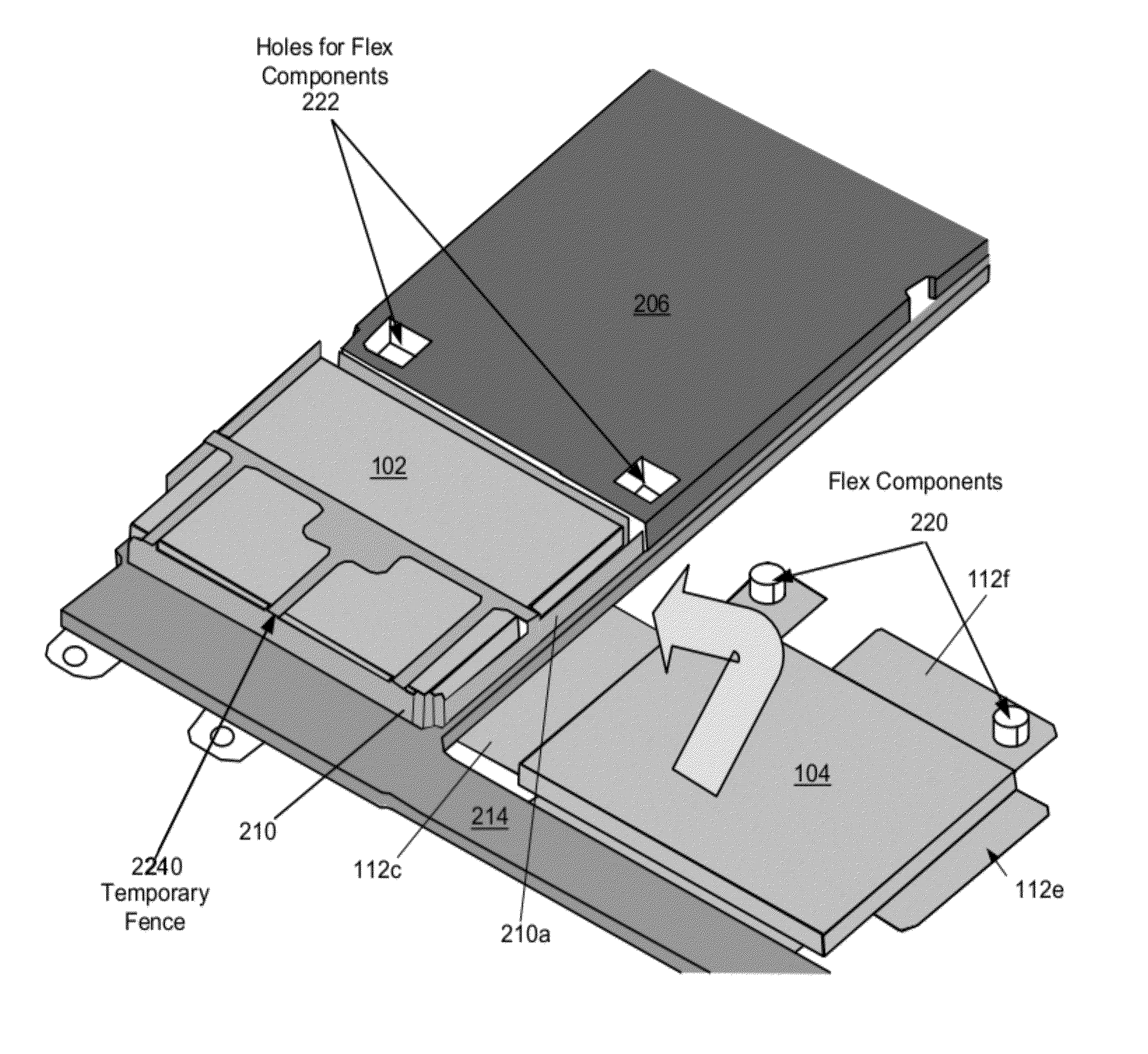
[0012]In one embodiment, the faraday cage can be used to block radio frequency (RF) signals generated by the chips from reaching an antenna installed in the portable computing device. The antenna can be a component of a wireless interface used on the device. Using the flexible circuit connector to form part of the faraday cage rather than a separate metal shield can result in a thinner and lighter weight design since the flexible circuit connector is thinner and weighs less than a typical metal component used for RF shielding. For example, stainless steel is typically used to form a faraday cage used in RF shielding. A flexible circuit connector can be about ⅙ the thickness of a stainless steel component used in this manner.

Problems solved by technology

The trend of smaller, lighter, more compact and powerful presents continuing challenges in the design portable computing devices and its associated components.

Method used


Image

  • Compact folded configuration for integrated circuit packaging
  • Compact folded configuration for integrated circuit packaging
  • Compact folded configuration for integrated circuit packaging

Examples


Embodiment Construction

[0029]In the following detailed description, numerous specific details are set forth to provide a thorough understanding of the concepts underlying the described embodiments. It will be apparent, however, to one skilled in the art that the described embodiments can be practiced without some or all of these specific details. In other instances, well known process steps have not been described in detail in order to avoid unnecessarily obscuring the underlying concepts.

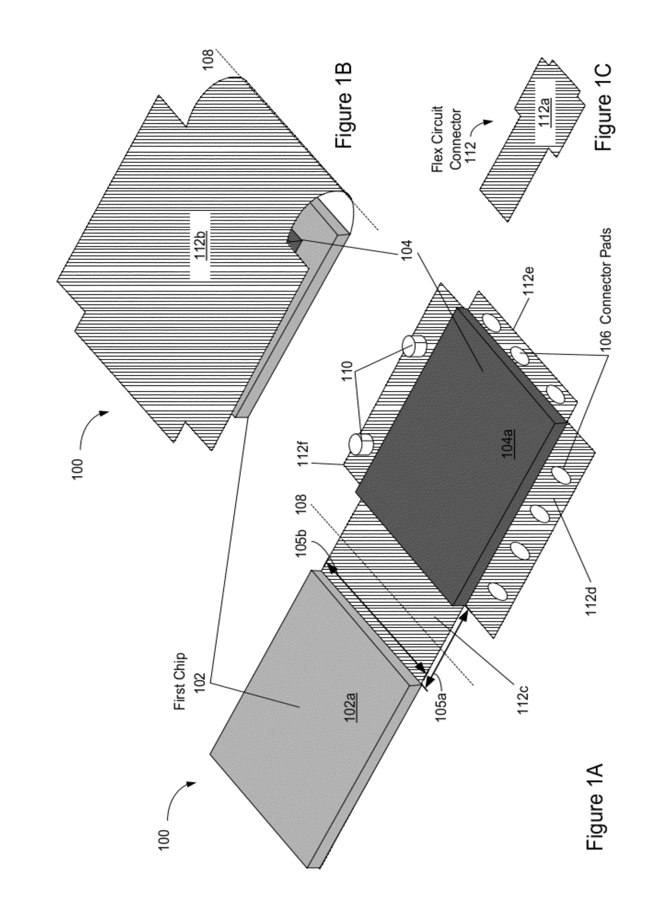
[0030]Broadly speaking, the embodiments disclosed herein relate to compact form factor integrated circuit packaging designs well suited for use in portable computing devices. For the remainder of this discussion and without loss of generality, the integrated circuits will be discussed in terms of memory devices such as FLASH memory devices, In particular, the FLASH memory devices can take the form of NAND type memory devices widely used in portable computing devices. The packaging designs take into consideration factors ...


PUM

PropertyMeasurementUnit
Flexibilityaaaaaaaaaa
Electrical conductoraaaaaaaaaa

Abstract

A memory unit for a computing device is described. The memory device can include a number of memory chips, such as flash nand chips, linked together via a flexible circuit connector. During installation of the memory device, portions of the flexible circuit connector can be bent or folded in different locations to allow an orientation of the memory chips to be changed relative to one another. In one embodiment, a memory device with a number of chips can be provided in a flat configuration and then can be folded to allow the chips to be installed in a stacked configuration. In another embodiment, the flexible circuit connector can be grounded to other conductive components to allow the flexible circuit connector to be used as part of a faraday cage surrounding the memory chips.

Description

BACKGROUND[0001]1. Field of the Invention[0002]The invention relates to packaging design for consumer electronic devices and more particularly, methods and apparatus for providing packaging and RF shielding configurations for memory chips used in consumer electronic devices.[0003]2. Description of the Related Art[0004]In recent years, portable computing devices such as laptops, PDAs, media players, cellular phones, etc., have become small, light and powerful. One factor contributing to this reduction in size can be attributed to the manufacturer's ability to fabricate various components of these devices in smaller and smaller sizes while in most cases increasing the power and or operating speed of such components. Another factor contributing to the reduction in size is that from a visual stand point, users often find compact and sleek designs of consumer electronic devices more aesthetically appealing and thus, demand compact and sleek designs. The trend of smaller, lighter, more co...

Claims


Application Information

Patent Timeline
IPC IPC(8): H05K7/02H01R43/00
CPCH01L2224/32225H01L24/81H01L25/50G06F1/1626H05K1/189H01L2225/06593Y10T29/49117H05K2201/10159H01L2225/06572H01L24/16H01Q1/526H04R3/00H05K2201/042H01Q1/243H01L2224/81801H01L2924/1438H01L2225/06558H01L23/552H01L2224/73203H05K1/0215H01L24/32H01L25/0657H05K2201/10371H01L24/73H01L2224/32145H01L2224/16225H01L23/5387H01L2924/1434G06F1/1684H04R2499/11H01L2924/14H01L2924/00
Inventor ROTHKOPF, FLETCHER R.HOBSON, PHILLIP M.MITTLEMAN, ADAMSHEDLETSKY, ANNA-KATRINA
Owner APPLE INC
Learn More