
Solid-State Thin-Film Capacitor

a thin-film capacitor and solid-state technology, applied in the field of solid-state electronics, can solve the problem that the substrate area devoted to the capacitor is not optimally available to support the formation of other electrical elements, and achieve the effect of reducing the overall size of the device and improving the functionality of the electronic devi

Active Publication Date: 2012-01-26
PROTEUS DIGITAL HEALTH INC
View PDF11 Cites 12 Cited by
  • Summary
  • Abstract
  • Description
  • Claims
  • Application Information

AI Technical Summary

Benefits of technology

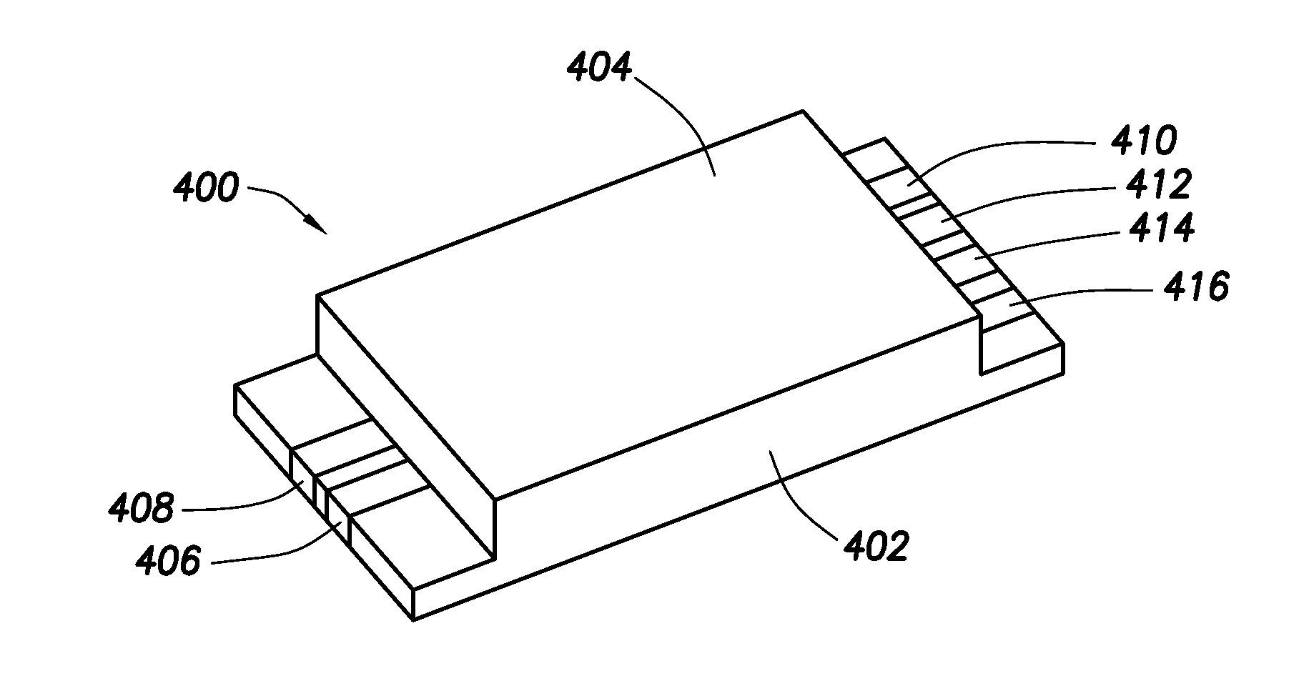
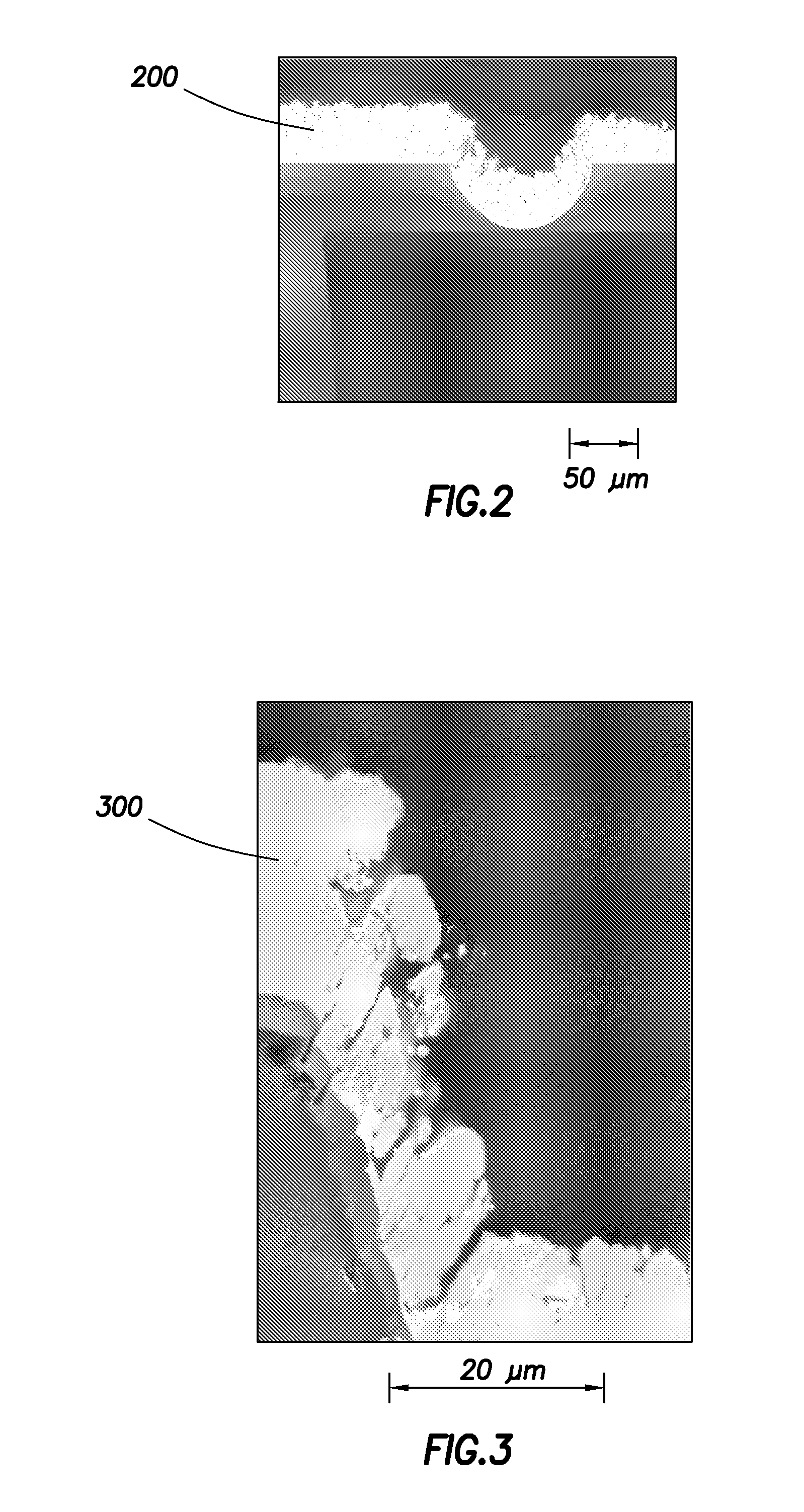
[0010]To achieve this object and other objects that will be made obvious in light of the present invention, provided are solid-state thin-film capacitors. Aspects of the solid-state thin-film capacitors include a multilayer structure made up of a first electrode layer of a transition metal, a dielectric layer of an oxide of the transition metal, and a second electrode layer of a metal oxide. Also provided are methods of making the solid-state thin-film capacitors, as well as devices that include the same. The present invention further enables the production of capacitive structures formed of thick, stress-free metallic structures on a semiconductor substrate, even within substrate locations having high aspect ratios. Furthermore, alternative embodiments of the present invention allow for the production of porous metallic structures and metallic layers displaying crenulations on a surface thereof. As such, the present invention allows for the production of semiconductor device designs that have not before been possible, thereby providing for significant improvements in electronic device functionality while decreasing the overall size of the device.

Problems solved by technology

Yet, prior art techniques applied to form a capacitor on a semiconductor substrate require that the substrate area devoted to the capacitor is not optimally available to support the formation of other electrical elements.

Method used


Image

  • Solid-State Thin-Film Capacitor
  • Solid-State Thin-Film Capacitor
  • Solid-State Thin-Film Capacitor

Examples


Embodiment Construction

[0029]Provided are solid-state thin-film capacitors. Aspects of the solid- state thin-film capacitors include a multilayer structure made up of a first electrode layer of a transition metal, a dielectric layer of an oxide of the transition metal, and a second electrode layer of a metal oxide. Also provided are methods of making the solid-state thin-film capacitors, as well as devices that include the same. As used herein, the term “solid-state” refers to a device or circuit that uses semiconductors rather than mechanical or vacuum tube circuits. Accordingly, the solid-state capacitors may have no moving parts, such that they have no mechanical action. In some instances, the solid-state capacitors are configured such that a current flowing through the capacitor flows from one electrode to the other electrode of the capacitor without flowing through a vacuum or a vacuum tube.

[0030]In further describing various aspects of the invention, designs and methods of manufacture and use of str...


PUM


Abstract

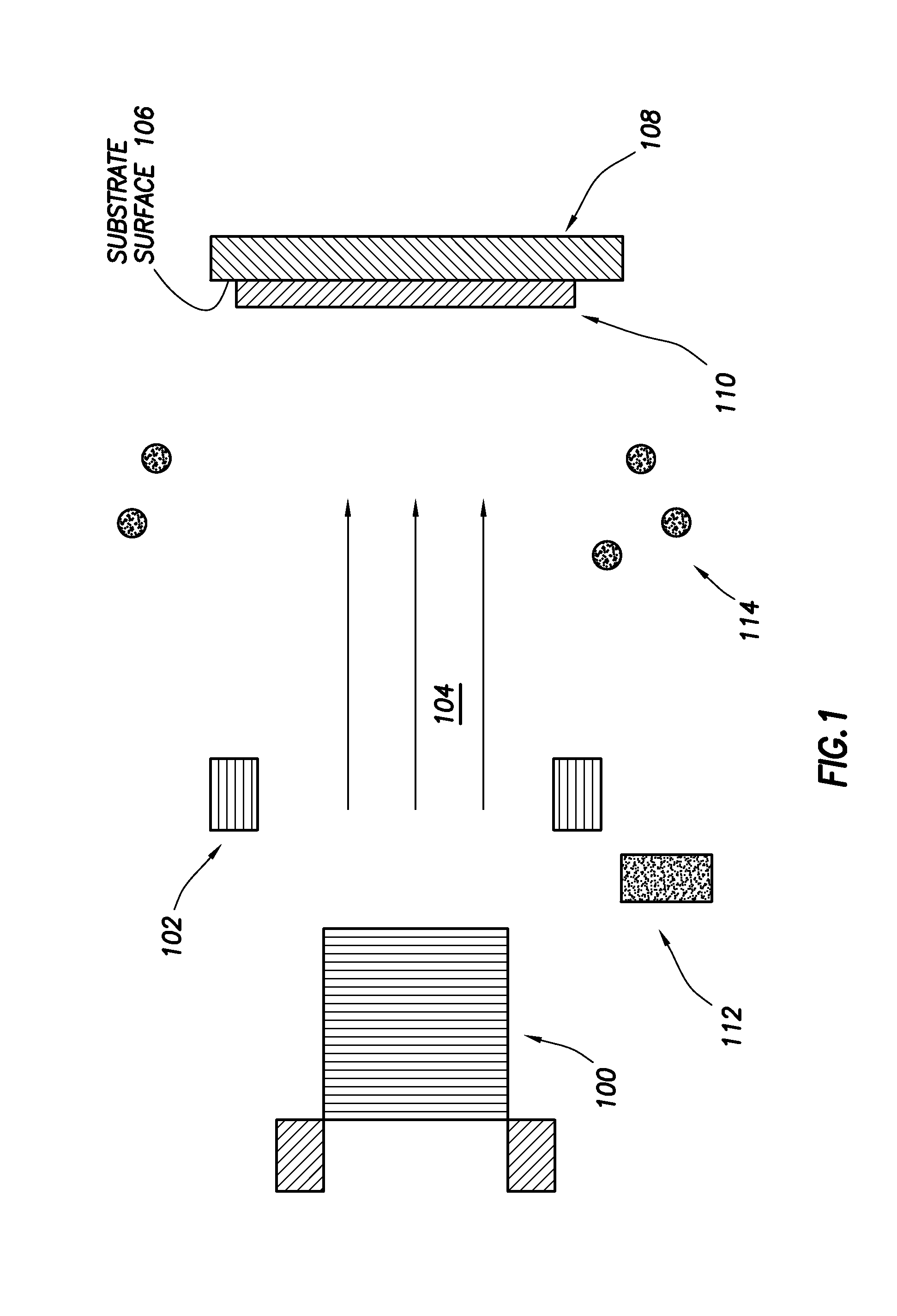
Solid-state thin-film capacitors are provided. Aspects of the solid-state thin-film capacitors include a first electrode layer of a transition metal, a dielectric layer of an oxide of the transition metal, and a second electrode layer of a metal oxide. Also provided are methods of making the solid-state thin-film capacitors, as well as devices that include the same. The capacitor may have one or more cathodic arc produced structures, i.e., structures produced using a cathodic arc deposition process. The structures may be stress-free metallic structures, porous layers and layers displaying crenulations. Aspects of the invention further include methods of producing capacitive structures using chemical vapor deposition and / or by sputter deposition.

Description

CROSS-REFERENCE TO RELATED APPLICATIONS[0001]Pursuant to 35 U.S.C. §119 (e), this application claims priority to the filing date of United States Provisional Patent Application Serial No. 61 / 228,027 (filed Jul. 23, 2009, titled “Solid-State Thin Film Capacitor”), the disclosure of which is herein incorporated by reference in its entirety.FIELD OF THE INVENTION[0002]The present invention relates to solid-state electronics. More particularly, the present invention relates to formation and use of capacitive structures on semiconductor substrates.BACKGROUND OF THE INVENTION[0003]Capacitors are passive electrical components that can store energy in an electric field between a pair of electrodes. Capacitors are often used in electronic circuits as energy-storage devices. A wide variety of different types of capacitors have been developed, including small electrolytic capacitors (for example as used in electronic circuits), basic parallel-plate capacitors, and mechanical variable capacitor...

Claims


Application Information

Patent Timeline
IPC IPC(8): H01L29/92H01L21/02
CPCH01G4/33
Inventor HAFEZI, HOOMAN
Owner PROTEUS DIGITAL HEALTH INC
Learn More