Method and Apparatus For Examining A Semiconductor Wafer

a semiconductor and apparatus technology, applied in semiconductor/solid-state device testing/measurement, instruments, television systems, etc., can solve the problems of untreated edge of silicon wafer sliced from a single crystal with a comparatively rough and non-uniform surface, source of disturbing particles, and spalling, so as to increase the meaningfulness of edge inspection and increase the risk of breaking

Inactive Publication Date: 2012-01-12
SILTRONIC AG
View PDF10 Cites 13 Cited by
  • Summary
  • Abstract
  • Description
  • Claims
  • Application Information

AI Technical Summary

Benefits of technology

[0009]Therefore, an object of the present invention was to increase the meaningfulness of the edge inspection and, in particular, to enable an unambiguous classification of the detected edge defects with regard to increased risk of breaking. These and other objects are achieved by means of a method for examining a semiconductor wafer, wherein the edge of the semiconductor wafer is examined by means of an imaging method and the positions and forms of defects on the edge are determined thereby, wherein, in addition, a ring-shaped region on the flat area of the semiconductor wafer, the outer margin of which region is not more distant than 10 mm from the edge, is examined by means of photoelastic stress measurement, and the positions of stressed regions in the ring-shaped region are determined, wherein the positions of the defects and the positions of the stressed regions are compared with one another, and the defects are classified in classes on the basis of their form and the results of the photoelastic stress measurement.

Problems solved by technology

The untreated edge of a silicon wafer sliced from a single crystal has a comparatively rough and non-uniform surface.
It often experiences spalling under mechanical loading and is a source of disturbing particles.
Therefore, defects and impressions on the edge cannot be completely avoided.
Some of these defects, such as, for example, cracks and spalling, can have the effect, for example, that the affected silicon wafers break in the course of further processing, particularly if additional stresses occur such as in the case of thermal processes or coatings in combination with mechanical treatments, which leads to considerable problems in the production line.
The previously known methods of edge inspection do not always yield sufficient information about the nature of the defects detected.
In particular, often it is not possible to identify whether a critical defect which can lead to the breaking of the semiconductor wafer is involved.
This means that sorting of the silicon wafers is beset by a considerable uncertainty.
The former factor decreases the yield unnecessarily, and the latter factor leads to problems for the customer.

Method used


Image

  • Method and Apparatus For Examining A Semiconductor Wafer
  • Method and Apparatus For Examining A Semiconductor Wafer
  • Method and Apparatus For Examining A Semiconductor Wafer

Examples


Embodiment Construction

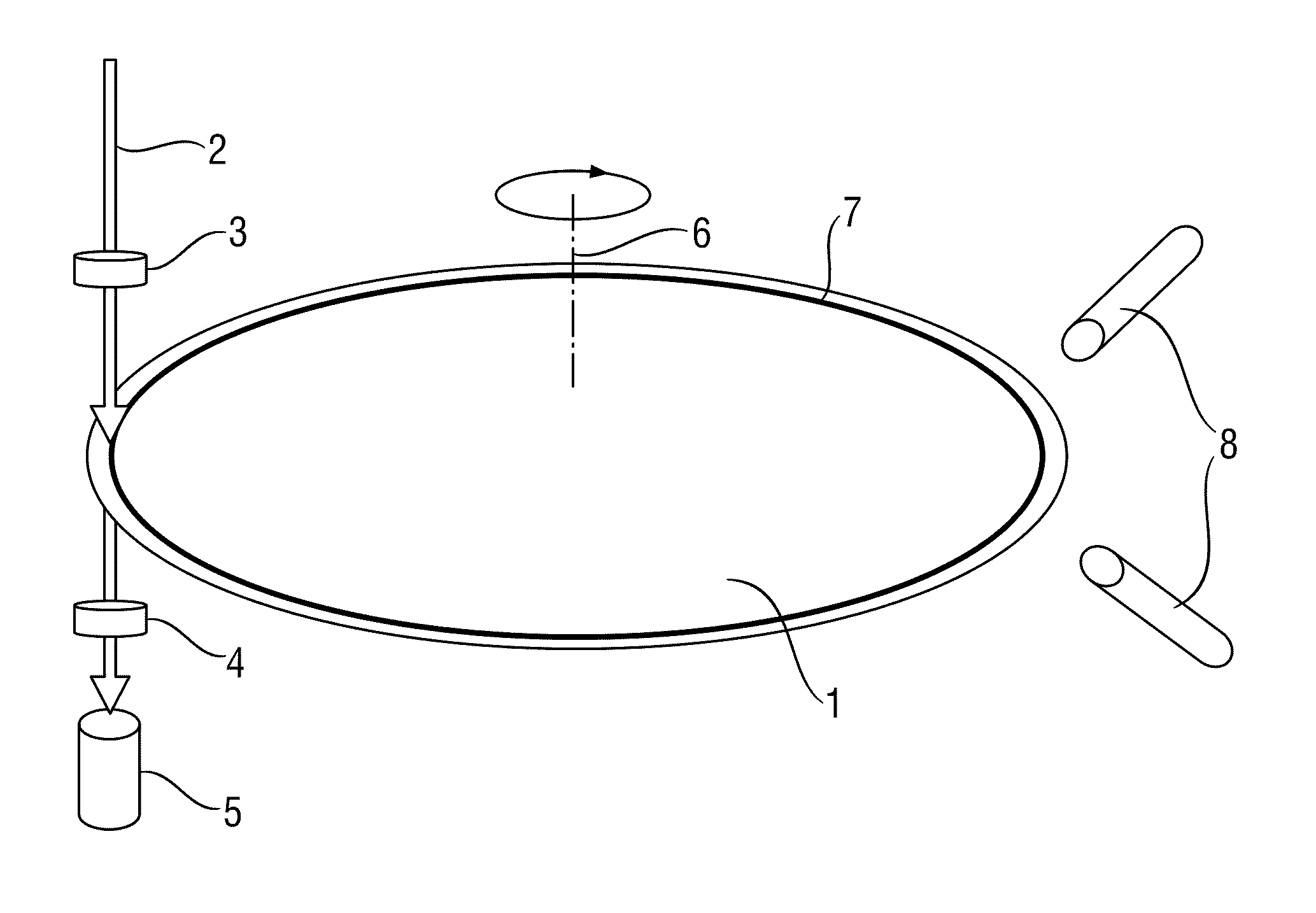
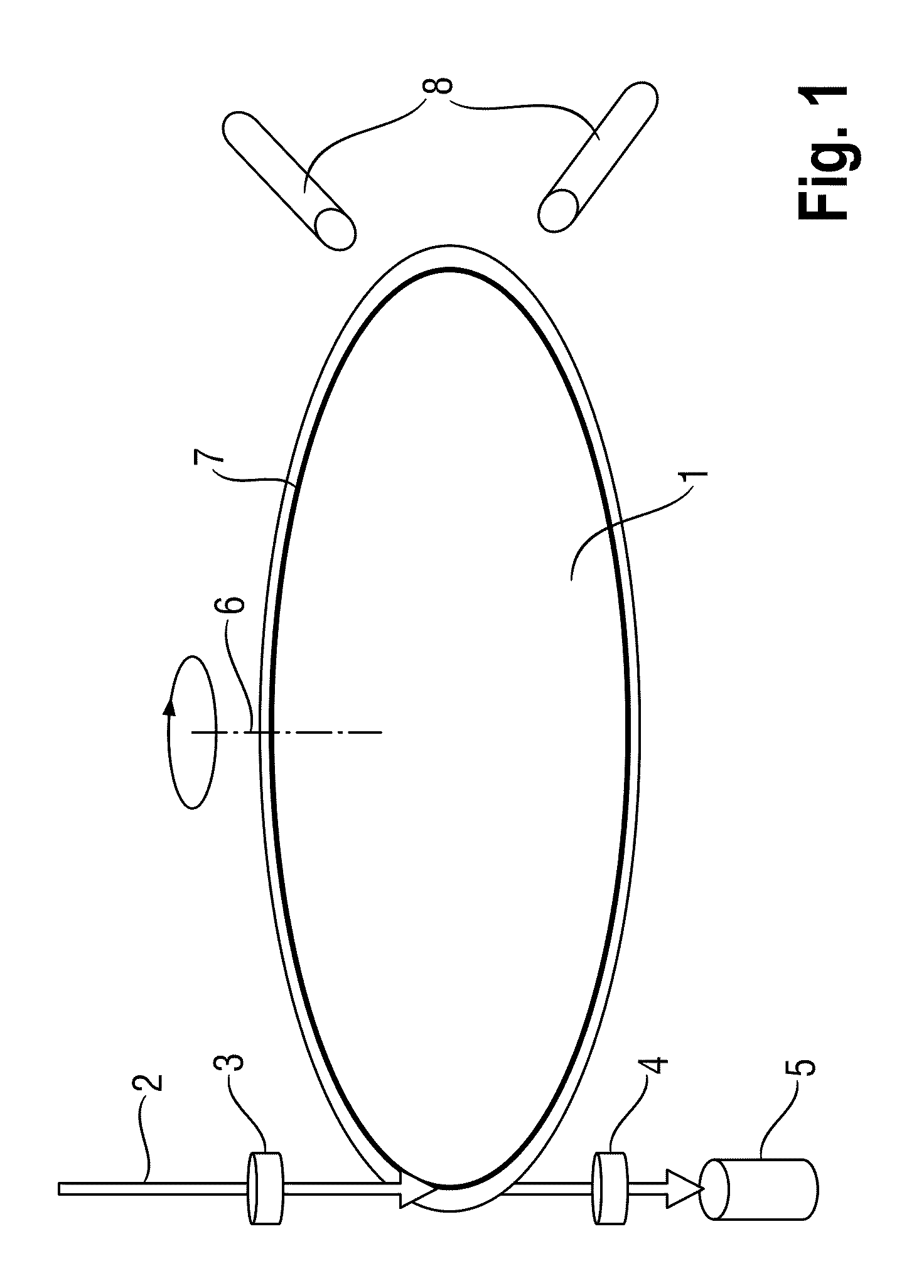
[0012]In contrast to the known methods for the detection and classification of edge defects, the method of the invention does not just use an imaging method, but rather combines the latter with data from a photoelastic stress measurement, i.e. with information about stressed regions in the material, in order to unambiguously identify edge defects that are critical with respect to breakage.

[0013]The imaging methods used can be optical imaging methods (using one or more cameras), electron-optical methods or atomic force microscopy (AFM).

[0014]Optical imaging methods examine the wafer edge by means of bright field or dark field optics or the combination of both. Typically, the wafer surface is examined on the front and rear sides in a region from the outermost margin of the wafer to approximately 5 mm inward, such that a sufficiently large overlap with the much more sensitive methods of front and rear side inspection arises in the edge region. The illumination of the wafer edge in brig...


PUM


Abstract

The edges of semiconductor wafers are examined by an imaging method and the positions and forms of defects on the edge are determined, and in addition, a ring-shaped region on the flat area of the semiconductor wafer, the outer margin of which is ≦10 mm from the edge, is examined by means of photoelastic stress measurement and the positions of stressed regions in the ring-shaped region are determined, wherein the positions of the defects and the positions of the stressed regions are compared with one another, and the defects are classified in classes on the basis of their form and the results of the photoelastic stress measurement.

Description

CROSS-REFERENCE TO RELATED APPLICATION[0001]This application claims priority to German Patent Application No. DE 10 2010 026 351.6 filed Jul. 7, 2010 which is herein incorporated by reference.BACKGROUND OF THE INVENTION[0002]1. Field of the Invention[0003]The invention relates to a method and an apparatus for examining a semiconductor wafer, wherein the edge of the semiconductor wafer is examined by means of an imaging method and the positions of defects on the edge are determined in this way.[0004]2. Background Art[0005]The quality requirements for the edges of semiconductor wafers, for example monocrystalline silicon wafers, are ever increasing, particularly in the case of large diameters (≧300 mm). In particular, it is intended for the edge to be as free as possible from contamination and other defects and to have a low roughness. Moreover, it is intended that the edges be resistant to increased mechanical stresses during transport and in process steps during the production of mi...

Claims


Application Information

Patent Timeline
IPC IPC(8): G06K9/00H04N7/18
CPCG01N21/9503H01L22/00
Inventor PASSEK, FRIEDRICHFUCHS, JUERGENHUBER, ANDREASLANGENFELD, FRIEDRICHLAUBE, FRANK
Owner SILTRONIC AG
Why Eureka
Try Eureka