
Semiconductor device and method for fabricating the same

a technology of semiconductor devices and semiconductor devices, applied in semiconductor devices, semiconductor/solid-state device details, electrical equipment, etc., can solve the problems of increased production costs and difficulty in securing a sufficient process margin, and achieve the effect of preventing a bridg

Active Publication Date: 2012-01-05
SK HYNIX INC
View PDF5 Cites 17 Cited by
  • Summary
  • Abstract
  • Description
  • Claims
  • Application Information

AI Technical Summary

Benefits of technology

The present invention is about a semiconductor device with a 6 F2 cell architecture that prevents bridges between active regions and ensures a margin of contact for a storage node contact plug. The semiconductor device includes a word line, a bit line, an active region arranged in an oblique direction at the word line and the bit line, and a contact pad contacting the active region. The contact pad extends in the oblique direction. The method for fabricating the semiconductor device includes forming an isolation layer in a substrate to define an active region arranged in a first direction, forming a word line in the substrate to cross the active region in an oblique direction, forming an interlayer dielectric layer over the entire surface of the substrate, forming a contact pad passing through the interlayer dielectric layer and contacting the active region, wherein the contact pad extends in the first direction, and forming a bit line crossing the word line.

Problems solved by technology

Accordingly, it is difficult to secure a sufficient process margin in forming the storage node contact plugs.
Accordingly, production cost may increase.

Method used


Image

  • Semiconductor device and method for fabricating the same
  • Semiconductor device and method for fabricating the same
  • Semiconductor device and method for fabricating the same

Examples


first embodiment

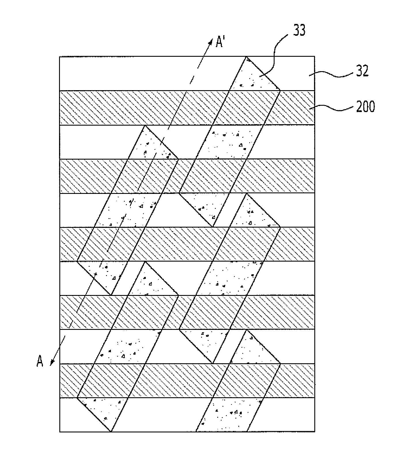
[0023]FIGS. 3A to 3E are plan views illustrating a method for fabricating a semiconductor device in accordance with the present invention. FIGS. 4A to 4E are cross-sectional views taken along lines A-A′ of FIGS. 3A to 3E, respectively.

[0024]Referring to 3A and 4A, an isolation layer 32 is formed in a substrate 31 to define a plurality of active regions 33. At this time, the active regions 33 may have such a structure that the major axis thereof is extended in an oblique direction at a buried gate and a bit line formed subsequently.

[0025]A plurality of buried gates 200 are formed in the substrate 31 so as to cross both of the isolation layer 32 and the active regions 33. The buried gates 200 serve as word lines. A method for forming the buried gates 200 is described in detail as follows.

[0026]First, a plurality of trenches 34 are formed in the substrate 31 so as to cross both of the isolation layer 32 and the active regions 33. A gate dielectric layer 35 is formed on the surface of e...

second embodiment

[0043]FIGS. 6A to 6E are plan views illustrating a method for fabricating a semiconductor device in accordance with the present invention. FIGS. 7A to 7E are cross-sectional views taken lines A-A′ of FIGS. 6A to 6E, respectively.

[0044]Referring to FIGS. 6A and 7A, an isolation layer 52 is formed in a substrate 51 to define a plurality of active regions 53. At this time, the active regions 53 may have such a structure that the major axis thereof is extended in an oblique direction at a buried gate and a bit line formed subsequently.

[0045]A plurality of buried gates 300 are formed in the substrate 51 so as to cross both of the isolation layer 52 and the active regions 53. The formation process of the buried gates 300 may be the same as the formation process of the buried gates 200 in accordance with the first embodiment of the present invention. Therefore, the detailed descriptions thereof are omitted here.

[0046]Referring to FIGS. 6B and 7B, a first interlayer dielectric layer 58 is f...


PUM


Abstract

A semiconductor device includes a word line, a bit line crossing the word line, an active region arranged in an oblique direction at the word line and the bit line, and a contact pad contacting the active region, where the contact pad extends in the oblique direction.

Description

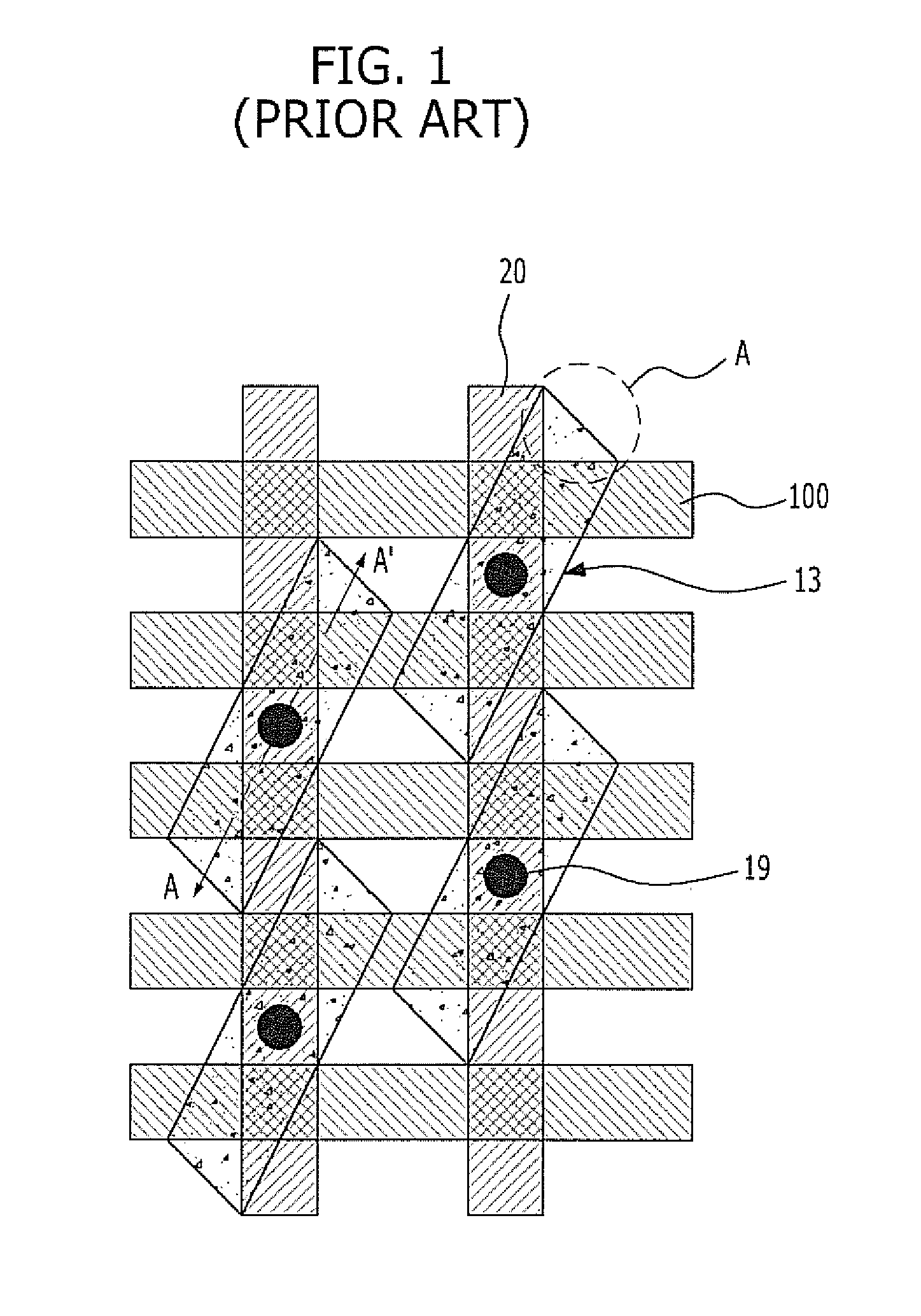
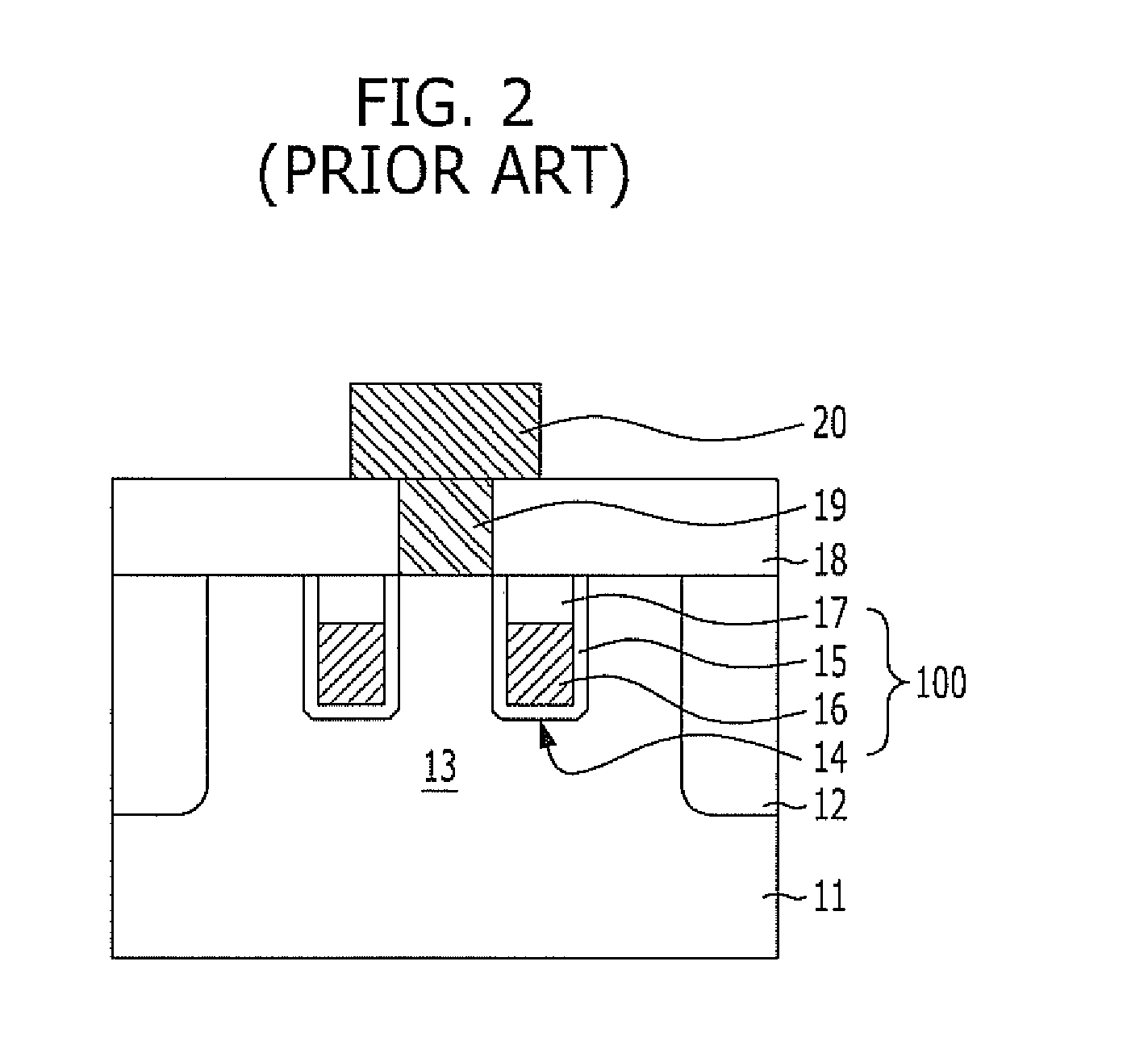
CROSS-REFERENCE TO RELATED APPLICATIONS[0001]The present application claims priority of Korean Patent Application No. 10-2010-0064461, filed on Jul. 5, 2010, which is incorporated herein by reference in its entirety.BACKGROUND[0002]1. Field[0003]Exemplary embodiments of the present invention relate to a technology for fabricating a semiconductor device, and more particularly, to a semiconductor device having a 6 F2 cell architecture and a method for fabricating the same.[0004]2. Description of the Related Art[0005]With the development of the fabrication technology of semiconductor devices, the size of the semiconductor devices has been reduced, and the integration degree thereof has been rapidly increased. A cell architecture of a memory device, such as DRAM (Dynamic Random Access Memory), changes from 8 F2 architecture to 6 F2 architecture, for higher integration. Here, F means a minimum critical dimension (CD) applied to the design rule of the memory device.[0006]FIG. 1 is a plan ...

Claims


Application Information

Patent Timeline
Patent Type & Authority Applications(United States)
IPC IPC(8): H01L23/48H01L21/768H10B12/00
CPCH01L27/10888H01L27/10855H10B12/0335H10B12/485H01L27/1222H10B12/00H10B12/30
Inventor KIM, DOO-KANGSEO, DAE-YOUNG
Owner SK HYNIX INC
Learn More