Manufacturing process for making photovoltaic solar cells

Inactive Publication Date: 2011-12-29
IBM CORP
View PDF4 Cites 3 Cited by
  • Summary
  • Abstract
  • Description
  • Claims
  • Application Information

AI Technical Summary

Benefits of technology

[0006]It is an object of the invention to provide a manufacturing process for a photovoltaic solar cell with improved efficiency by reducing degradation of a dielectric layer on a rear side of the solar cell.
[0009]Preferably, a deterioration of the dielectric layer while establishing an electrical contact between the solar cell body, e.g. p-doped Si, and the metallic contacts can be avoided. The metallic contact does not need to penetrate the dielectric layer; thus, harsh conditions usually necessary for penetration of aluminum through the dielectric layer are not necessary. A firing step can be performed together with a front side contact annealing step, thus reducing the thermal load of the solar cell during manufacture.
[0010]It is possible to integrate the back contact manufacturing process steps into a given process flow of the manufacture of a solar cell and can easily comply with requirements of a volume production of solar cells.
[0015]In an expedient development, the passivation layer may be deposited anisotropically so that a passivation layer thickness deposited on sidewalls of the metal contacts is thinner than a passivation layer thickness on a front surface of the metal contacts. The passivation layer can be deposited on the complete rear surface without masking. Even if the passivation layer covers the rear side, portions of the passivation layer on the metal contacts can be bypassed by embedding such portions in the metal contacts and / or in the metallic layer forming the backside field. Advantageously, the layer thickness of the passivation layer can be established in a way to comply with requirements of antireflection conditions. Particularly, the layer thickness can be large enough so as to achieve sufficient antireflection properties of the passivation layer. On the other hand, the passivation layer deposited on the sidewalls can be removed easier than on the front surface of the metal contacts.

Problems solved by technology

When forming the aluminum back contact, a degradation of the dielectric layer may decrease the efficiency of the solar cell by typically 1%-1.5%.

Method used


Image

  • Manufacturing process for making photovoltaic solar cells
  • Manufacturing process for making photovoltaic solar cells
  • Manufacturing process for making photovoltaic solar cells

Examples


Embodiment Construction

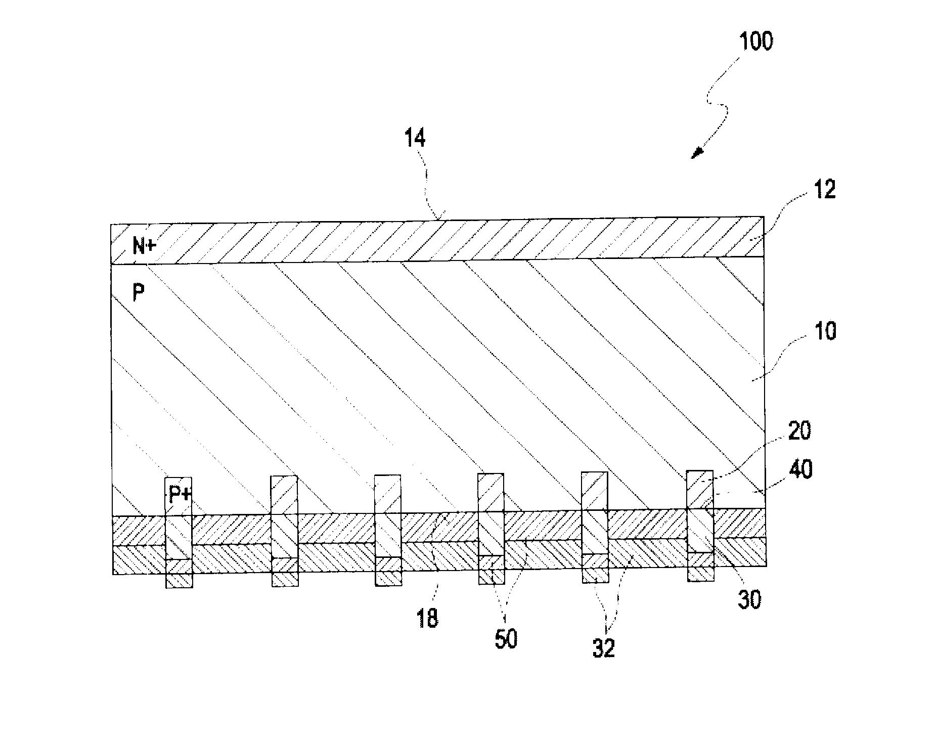
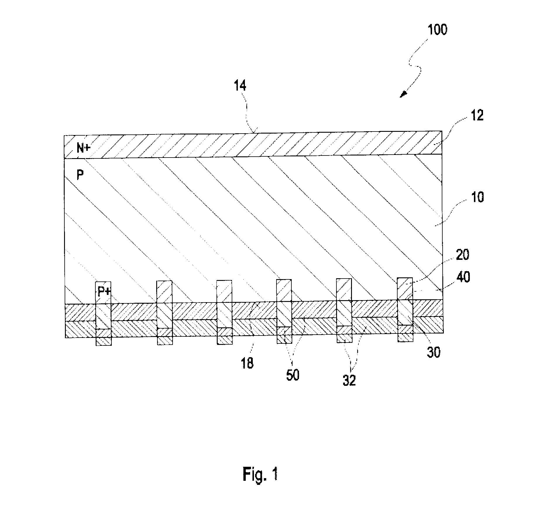
[0030]FIG. 1 depicts a cross section of a solar cell 100 manufactured with the inventive manufacturing process. The solar cell 100 comprises a semiconductor body 10, where the bulk material is typically lightly p-doped and a high doped n+-layer12 on its front surface 14 forming a p / n junction close to the front surface 14.

[0031]On the rear side 18 of the semiconductor body 10, localized high doped (p++) areas 20, i.e. boron doped, are arranged in the semiconductor body 10. On top of the high doped areas 20 metal contacts 30 are formed having an interface 40. A passivation layer 50 is arranged between the localized metal contacts 30. On top of the passivation layer 50 a metal layer 32 is arranged, covering the passivation layer 50, as well as the metal contacts 30. As a result, portions of the passivation layer 50 that are arranged on the metal contacts 30 are embedded in the metal layer 32.

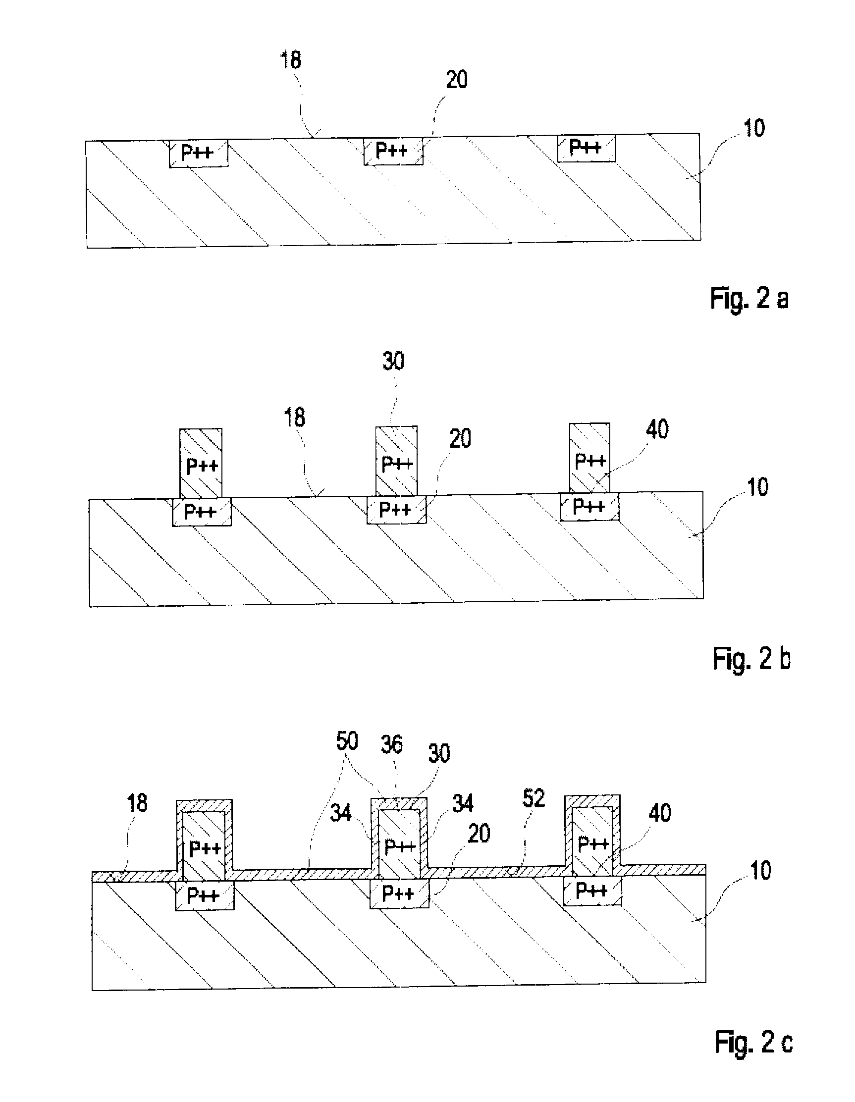
[0032]FIGS. 2a through 2c illustrate first process steps for forming metal contacts 30 on high...


PUM


Abstract

The invention relates to a manufacturing process of a photovoltaic solar cell (100) comprising:providing high doped areas (20) on the rear side (18) of the photovoltaic solar cell (100),providing localized metal contacts (30) localized on said high doped areas (20),providing a passivation layer (50) covering a surface (52) between said contacts (30), wherein the contacts (30) remain substantially free of the passivation layer (50), anddepositing a metal layer (32) for a back surface field.

Description

RELATED APPLICATION[0001]This application is based on and claims the benefit of Priority from European Patent Application 10167298, filed Jun. 25, 2010.FIELD OF THE INVENTION[0002]The invention relates to a manufacturing process for making photovoltaic cells, more particularly for making back contacts of photovoltaic solar cells.BACKGROUND OF THE INVENTION[0003]Solar cell products usually comprise a semiconductor substrate, preferably a silicon substrate with a photoactive p-n-junction, on a front surface being covered with a contact grid comprising stripes and finger-like structures, and a rear side with an electrical contact covering the entire rear side of the solar cell. The rear side is often prepared with screen printing methods.[0004]In US 2009 / 0110808 A1 a manufacturing process is disclosed for preparing back contacts and surface fields on the rear side of a photovoltaic solar cell. Molten aluminum is used to form the contact regions by utilizing a spraying method, which may...

Claims


Application Information

Patent Timeline
IPC IPC(8): H01L31/18
CPCY02E10/547H01L31/02167H01L31/1804H01L31/068H01L31/022425Y02P70/50
Inventor KRAUSER, RANIERCLEVENGER, LAWRENCE A.PRETTYMAN, KEVINSAPP, BRIAN CHRISTOPHERPETRARCA, KEVIN S.HOVEL, HAROLD JOHNPFEIFFER, GERDLI, ZHENGWENRADENS, CARL JOHN
Owner IBM CORP
Why Eureka
Try Eureka