
Light pipe etch control for CMOS fabrication

a technology of metal oxidesemiconductor and fabrication, applied in the direction of basic electric elements, solid-state devices, electric devices, etc., can solve the problems of cmos sensor depth fluctuations, lps variations, and the size of each pixel sensor,

Active Publication Date: 2011-12-29
HIMAX IMAGING LIMITED
View PDF2 Cites 38 Cited by
  • Summary
  • Abstract
  • Description
  • Claims
  • Application Information

AI Technical Summary

Benefits of technology

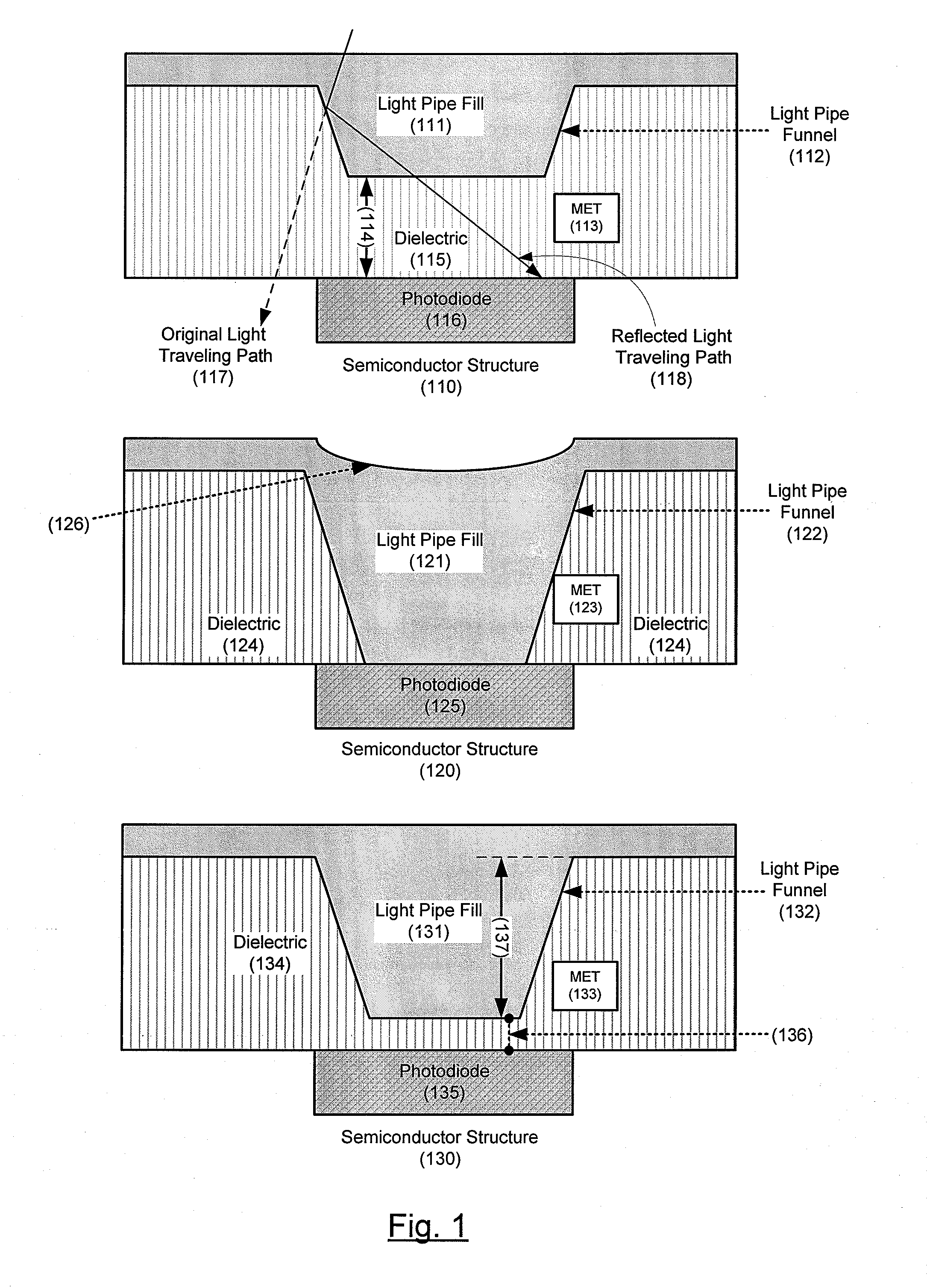
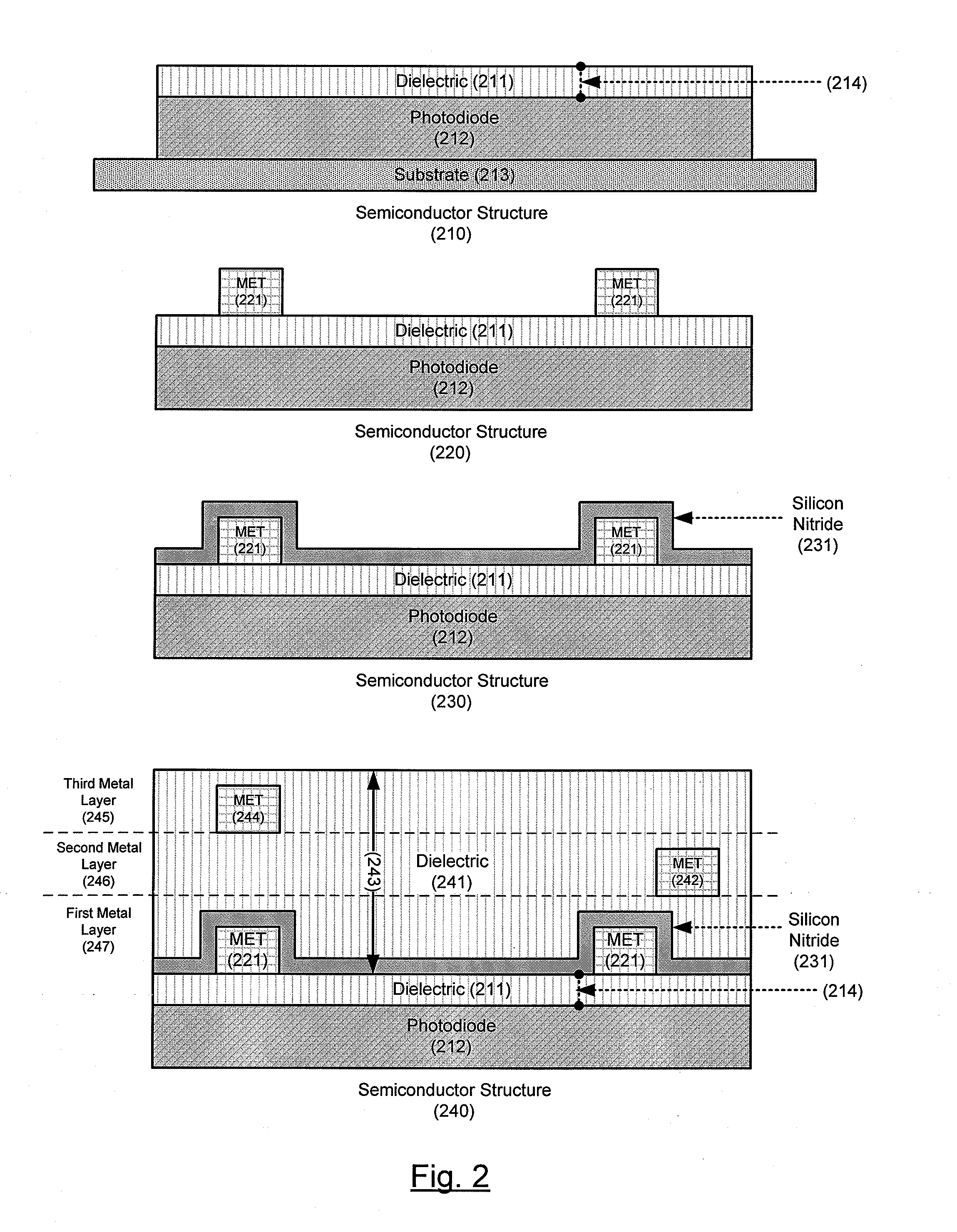
"The present disclosure relates to methods and semiconductor structures for fabricating a light pipe (LP) on a semiconductor substrate for a complementary metal-oxide-semiconductor (CMOS) image sensor. The technical effects of the disclosure include improving the light sensitivity and angular response of the pixel sensor by implementing a LP on top of the photodiode. The method includes depositing layers of material on the semiconductor substrate and etching them to create the desired semiconductor structure. The resulting semiconductor structure has a shallow or deep funnel-shaped LP, depending on the requirements of the pixel sensor. The desired LP has a desired height and thickness for better angle response and dark performance. The disclosure provides a detailed description of the fabrication process and the various semiconductor structures that can be created using this method."

Problems solved by technology

As the resolution of a CMOS image sensor increases, the size of each pixel sensor in the image sensor shrinks, which may also lead to the decreasing of the size of the photosensitive element (e.g., photodiode) in each pixel sensor.
However, conventional LP fabrication processes often lead to depth fluctuations and size variations for the LPs in the CMOS sensor.
The LPs built by these conventional fabrication processes may lead to low quality pixel sensors having poor light sensitivity and poor angular response.

Method used


Image

  • Light pipe etch control for CMOS fabrication
  • Light pipe etch control for CMOS fabrication
  • Light pipe etch control for CMOS fabrication

Examples


Embodiment Construction

[0011]In the following detailed description, reference is made to the accompanying drawings, which form a part hereof. In the drawings, similar symbols typically identify similar components, unless context dictates otherwise. The illustrative embodiments described in the detailed description, drawings, and claims are not meant to be limiting. Other embodiments may be utilized, and other changes may be made, without departing from the spirit or scope of the subject matter presented here. It will be readily understood that the aspects of the present disclosure, as generally described herein, and illustrated in the Figures, can be arranged, substituted, combined, and designed in a wide variety of different configurations, all of which are explicitly contemplated herein.

[0012]This disclosure is drawn, inter alia, to methods and semiconductor structures related to the fabricating of a LP on a semiconductor substrate. Throughout the disclosure, the term “light pipe” may broadly refer to a...


PUM


Abstract

In accordance with at least some embodiments of the present disclosure, a process for fabricating a light pipe (LP) is described. The process may be configured to construct a semiconductor structure having an etch-stop layer above a photodiode region and a first dielectric layer above the etch-stop layer. The process may be configured to etch a LP funnel through the first dielectric layer. And the process may be further configured to stop the etching of the LP funnel upon reaching and removing of the etch-stop layer.

Description

BACKGROUND OF THE DISCLOSURE[0001]1. Field of the Disclosure[0002]Embodiments of the present disclosure relate generally to complementary metal-oxide-semiconductor (CMOS) fabrication and more specifically to the fabricating of a light pipe for a CMOS image sensor.[0003]2. Description of the Related Art[0004]Unless otherwise indicated herein, the approaches described in this section are not prior art to the claims in this application and are not admitted to be prior art by inclusion in this section.[0005]Image sensors have great usages in many fields. CMOS image sensors generally consume less power and also cost less than charge-coupled devices (CCD) image sensors. As the resolution of a CMOS image sensor increases, the size of each pixel sensor in the image sensor shrinks, which may also lead to the decreasing of the size of the photosensitive element (e.g., photodiode) in each pixel sensor. As the CMOS image sensors become increasingly more sophisticated, the requirements of pixel ...

Claims


Application Information

Patent Timeline
Patent Type & Authority Applications(United States)
IPC IPC(8): H01L31/0232H01L31/18
CPCH01L27/14629H01L27/14685H01L27/14645
Inventor KIM, KIHONG
Owner HIMAX IMAGING LIMITED
Learn More