
Compensation of parasitic capacitances of capacitive sensors

a capacitance compensation and capacitance technology, applied in the field of capacitance compensation of parasitic capacitances of capacitive sensors, to achieve the effect of strong output signals

Inactive Publication Date: 2011-12-08
DIGITAL IMAGING SYST
View PDF0 Cites 4 Cited by
  • Summary
  • Abstract
  • Description
  • Claims
  • Application Information

AI Technical Summary

Benefits of technology

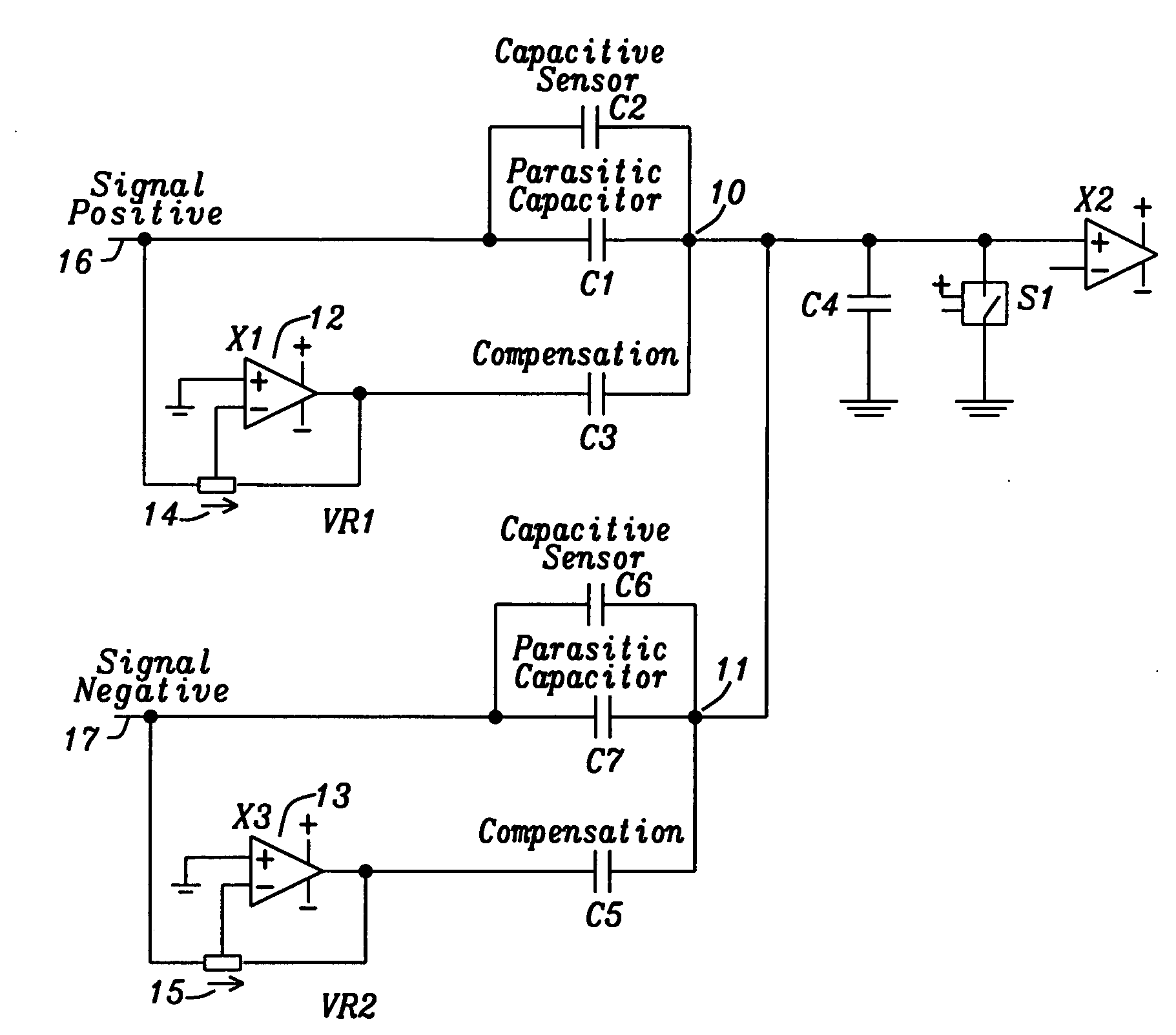
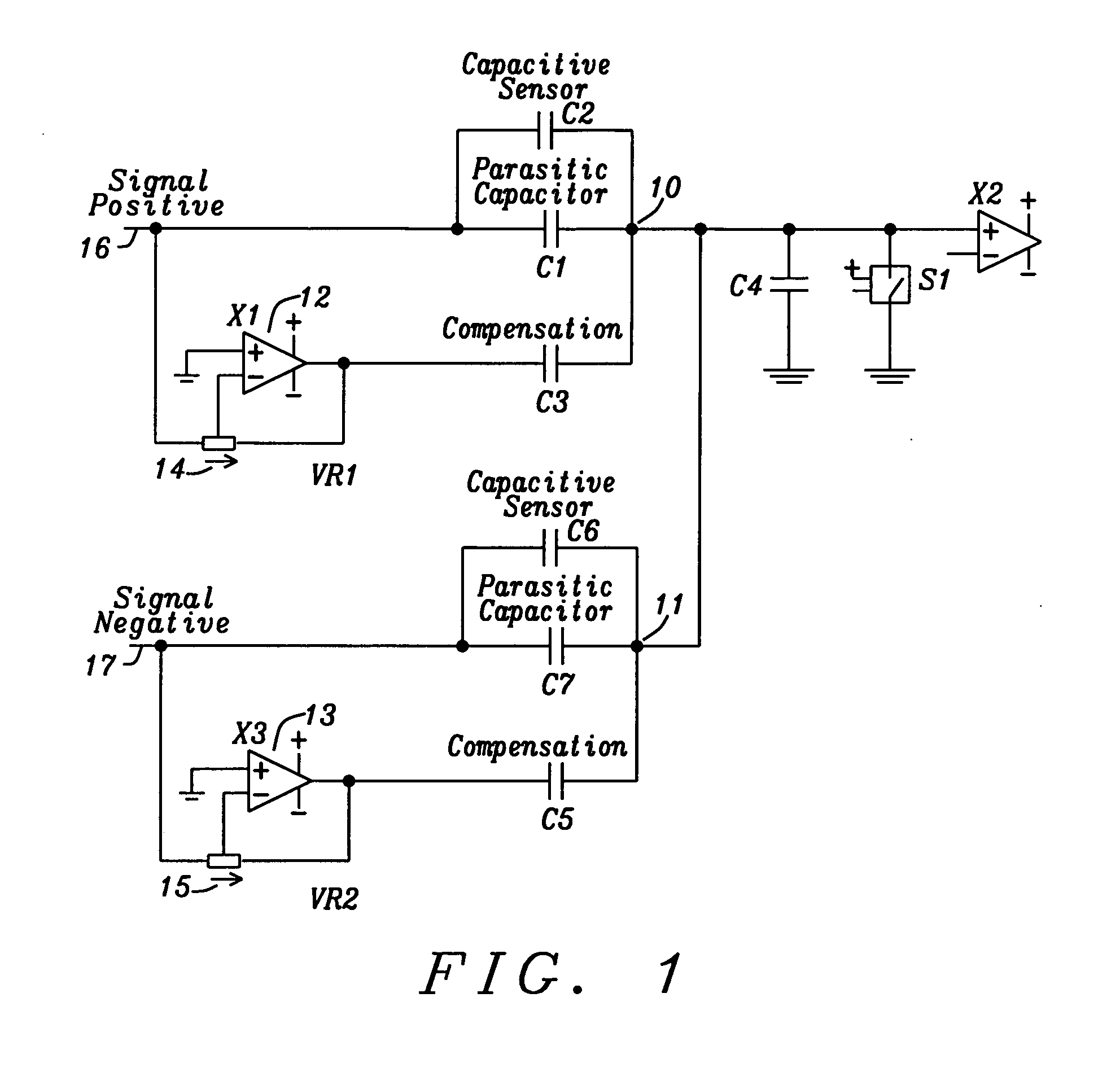
"The present invention provides a method and circuit to compensate for the impact of parasitic capacitances on capacitive sensors. The method involves charging compensation capacitors with a same but inverted charge as the related parasitic capacitances and neutralizing the charges of the parasitic capacitances by a switch. The circuit includes one or more capacitive sensors, a digital-to-analog converter, and a compensation capacitor in parallel with each sensor. The method and circuit can effectively improve the output signals of capacitive sensors and reduce the impact of parasitic capacitances."

Problems solved by technology

A drawback to capacitive sensors, especially those operating with small values / changes of capacitances is parasitic capacitances, which can heavily influence accuracy of capacitive sensors.

Method used


Image

  • Compensation of parasitic capacitances of capacitive sensors
  • Compensation of parasitic capacitances of capacitive sensors
  • Compensation of parasitic capacitances of capacitive sensors

Examples


first embodiment

[0025]FIG. 1 illustrates a block diagram showing the principal building blocks of a circuit invented compensating parasitic capacitances. A pair of capacitive sensors C2 and C6 is used to determine a position of an object, carrying one or more sensor plates that are to be moved to a target position. It should be noted that one or two or more than two capacitive sensors could be used with the present invention. Each sensor with a odd number (first, third, fifth, . . . sensor) has its first terminal connected to a positive input signal, each sensor with an even number (second, fourth, sixth . . . sensor) has its first terminal connected to a negative input signal, and all second terminals are connected to a common signal output.

[0026]Two sensor capacitors have been deployed in the preferred embodiment to enable a differential measurement of the position of the moving object. Each sensor capacitor has at least one plate on the moving object and one plate having a fixed position. Parasi...

second embodiment

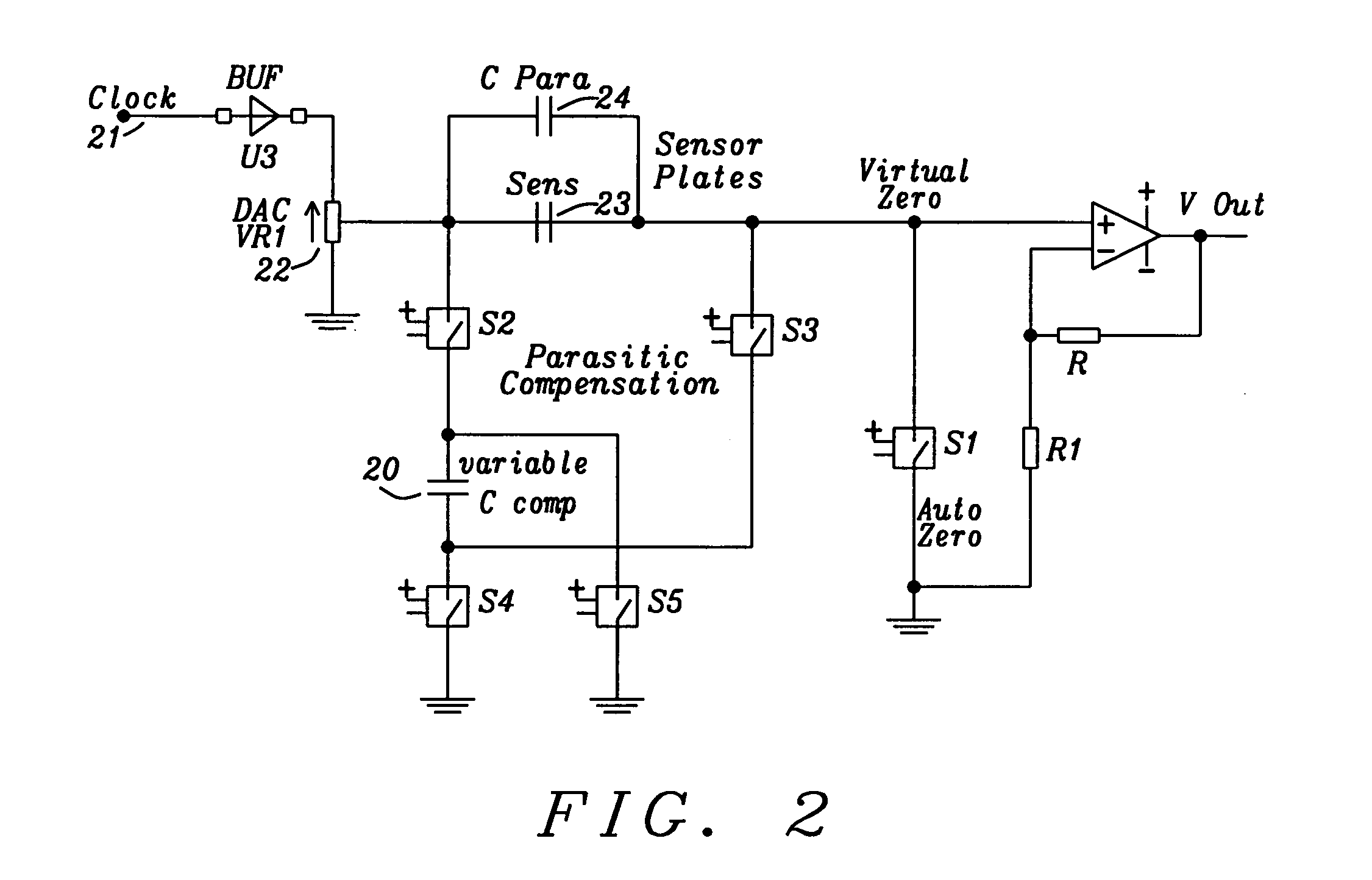
[0033]FIG. 2 illustrates a block diagram showing the principal building blocks of a circuit invented compensating parasitic capacitances. In this embodiment one sensor capacitor is used, it should be noted that two or more sensor capacitors could also be deployed with the type of embodiment of FIG. 2.

[0034]No operational amplifiers, as disclosed in FIG. 1 are used, but a variable compensation capacitor 20 is deployed. The variable capacitance has been achieved by using a capacitor array for adjustment. The operational capacitance of the compensation capacitor corresponds to the parasitic capacitance.

[0035]The capacitive array is adjusted by maximizing the output signal while moving the plate from one side to the other or have it set to one side at least. A maximum delta signal indicates that the parasitic capacitances are cancelled.

[0036]Furthermore FIG. 2 shows a capacitive sensor 23 and a parasitic capacitance is indicated by numeral 24. As in FIG. 1 another parasitic capacitance ...


PUM


Abstract

Circuits and methods for compensating the impact of parasitic capacitances on capacitive sensors have been achieved. The charge of a compensation capacitor assigned to each capacitive sensor is used to neutralize the charge of the parasitic capacitor.

Description

RELATED APPLICATION[0001]This application is related to the following US patent applications:DI08-002, titled “Distance measurement with capacitive sensor”, Ser. No. 12 / 290,386, filing date Oct. 30, 2008, andDI08-006, titled “Camera Shutter and position control thereof”, Ser. No. 12 / 658,280, filing date Feb. 5, 2010,and the above applications are assigned to the same assignee and are herein incorporated by reference in its entirety.BACKGROUND OF THE INVENTION[0002](1) Field of the Invention[0003]This invention relates generally to the field of capacitive sensors and relates more specifically to compensation of parasitic capacitances of capacitive sensors.[0004](2) Description of the Prior Art[0005]Capacitive sensors are capacitors separated by a dielectric material; often the electrodes used have the form of plates. Using the properties and knowledge of electric field and capacitance between separated charged electrodes / plates it is possible to retrieve information about distance, p...

Claims


Application Information

Patent Timeline
Patent Type & Authority Applications(United States)
IPC IPC(8): G01R27/26
CPCG01D5/24G01R29/24G01R27/2605
Inventor KRONMUELLER, FRANKKNOEDGEN, HORST
Owner DIGITAL IMAGING SYST
Learn More