
Selective solar absorbent coating and manufacturing method

Inactive Publication Date: 2011-10-13
ABENGOA SOLAR NEW TECH SA
View PDF8 Cites 28 Cited by
  • Summary
  • Abstract
  • Description
  • Claims
  • Application Information

AI Technical Summary

Benefits of technology

This invention seeks to resolve all the difficulties set out above, as each of the cermets layers are replaced by an alternating multilayered dielectric and metal structure, with very think layers, less than 10 nm and mainly under 1 nm. Dielectric layers are deposited through reactive sputtering, including inert gas and reactive gas in the chamber or part of the chamber where dielectric coatings are deposited. Metal layers are deposited through DC sputtering, introducing inert gas exclusively in the chamber or part of the chamber where metallic layers are deposited. As a result, precise control of the stoichiometry process is not required, since the depositing of the dielectric layers requires a composition of gases that guarantees the total reaction of the evaporated metal, while the metal nature of the alternating layers is determined by the inert gas introduced as process gas. As the depositing of both types of materials is realised in different chambers or in isolated parts of the same deposition chamber, gas mixture is minimal and no chemical reaction of the constituent material of the metal layers is produced. Likewise, as the deposition of dielectric and metal layers is realised in different places and with different gas compositions, there is no limit to the composition of dielectric and metallic layers, which can even be taken from the same batch of metal, forming dielectric layers from a metal element, such as oxides or nitrides of a metal, and metal layers of the same element.
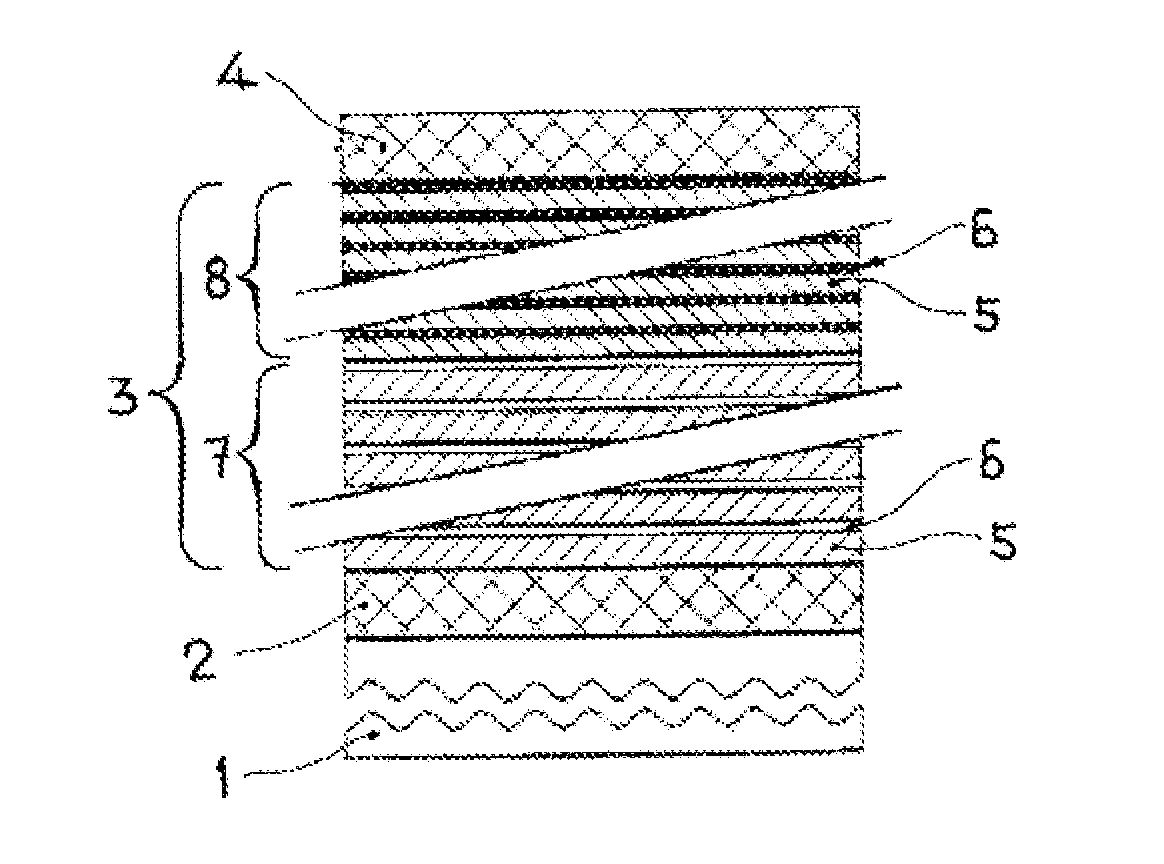
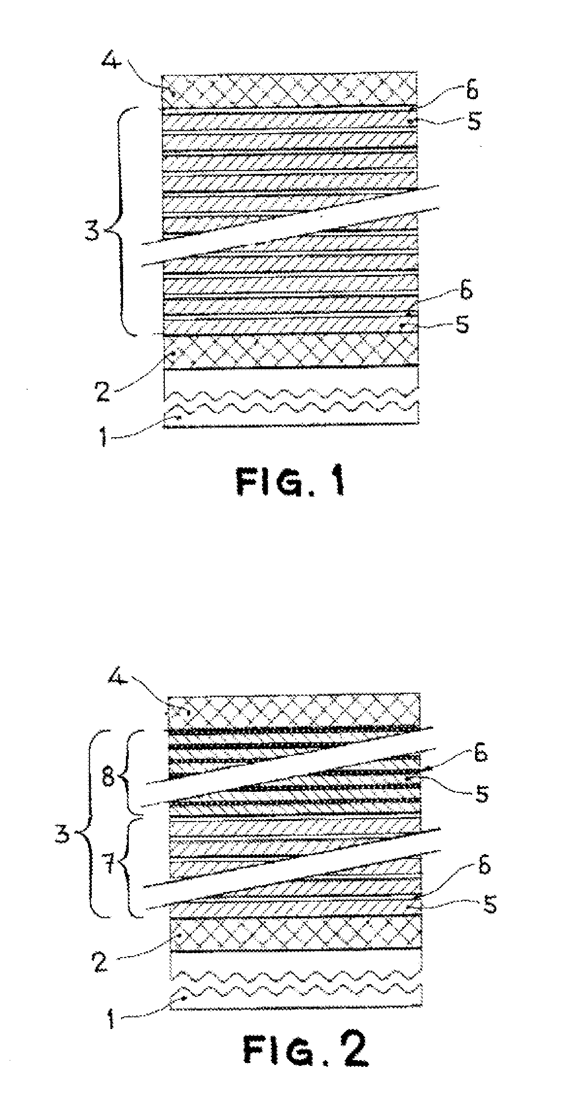
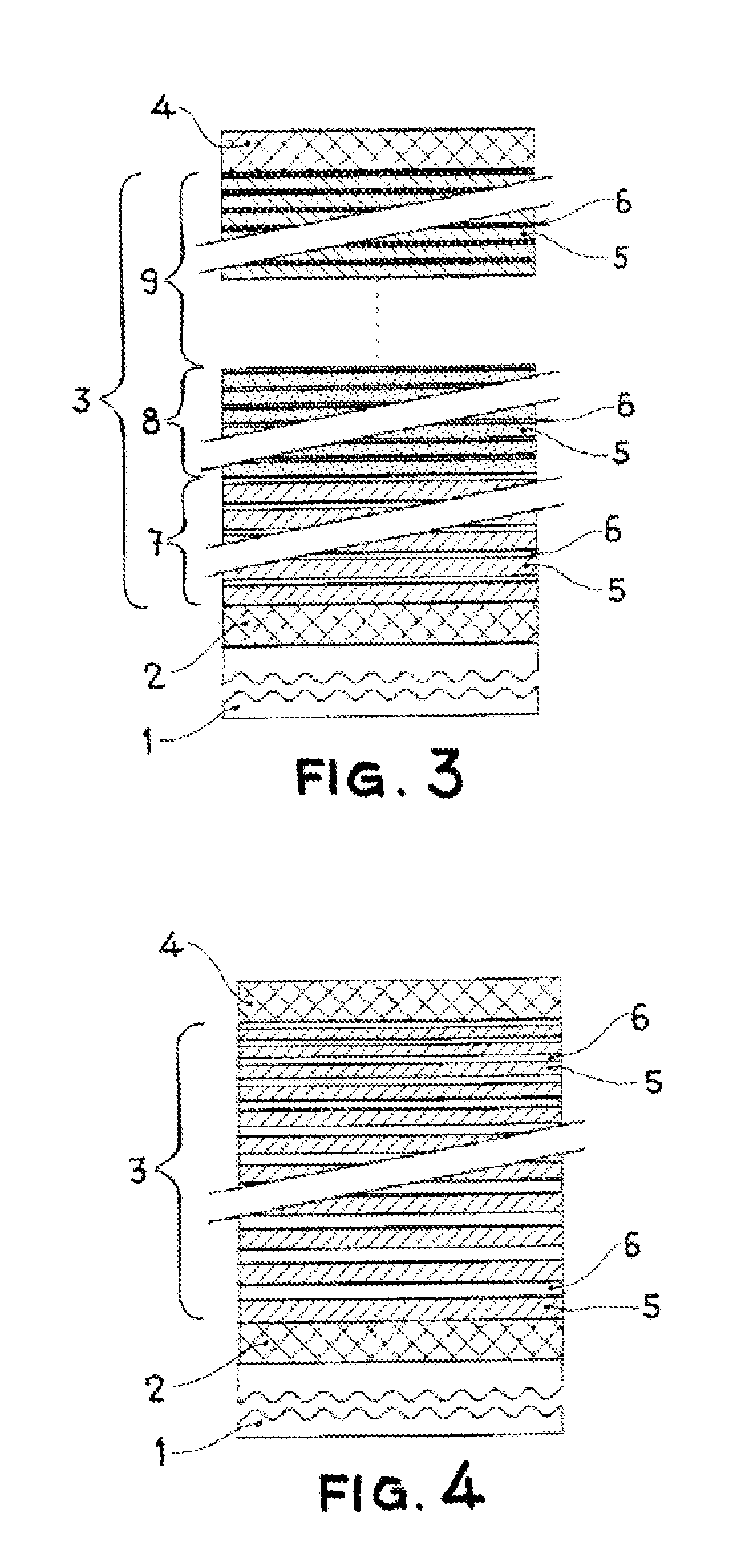
The selective solar coating in this invention is designed to absorb solar energy and transform it into heat with low emissivity properties, facilitating and making the manufacturing process more robust and reliable and allowing greater possibilities for its design and optimisation. The coating deposited on the substrate, which can be metallic or dielectric, ensures the mechanical and thermal stability of the coating, and is essentially characterised by including:At least one highly reflective metallic layer in far infrared (spectral range between 5 and 50 μm wave length) that provides low emissivity characteristics of the coating deposited on the substrate.A multilayered structure deposited on the reflective layer, that provides solar radiation absorbing properties, formed by alternating metallic and dielectric layers of a very small thickness (less than 10 nm and generally less than 1 nm), that can be homogenous for metallic layers, on the one hand, and dielectric, on the other, throughout the structure, differentiated in various zones or with thicknesses that gradually vary along the structure.At least one dielectric layer deposited on the absorbing multilayered structure that acts as an antireflective layer.
This invention also has the benefit that the coating can be used in capture systems at solar tower-type thermoelectric power plants, in which solar energy reflected by a multitude of heliostats is concentrated in the capture system positioned in a tower.

Problems solved by technology

The stoichiometry process is conditioned by the composition and partial pressures of the gases in the vacuum chamber in relation to the reactive gas consumption, and therefore depends on the evaporation speed, that is, cathode power, of its state, making accurate control of the stoichiometry process very difficult, requiring certain feedback mechanisms that can negatively affect the properties of the coatings.
Likewise, part of the codopant metal also reacts with the reactive gas and forms dielectric compounds, so this metal does not therefore contribute to the absorption of the layer and requires large concentrations of codopant metal.
Besides, this technique also presents limitations when choosing codopant metals as they should possess much less affinity for the reactive gas than the principal metal that forms the dielectric compound.

Method used


Image

  • Selective solar absorbent coating and manufacturing method
  • Selective solar absorbent coating and manufacturing method
  • Selective solar absorbent coating and manufacturing method

Examples


example 1

Selective Absorbing Coating with Absorbent Structure of Two Zones Based on Molybdenum (Mo) and Aluminium Silicon Oxide (SiAIOx)

On a substrate (1) of stainless steel 304 a layer of Mo of 300 nm is deposited. On this layer of Mo the absorbent multilayer structure consisting in two differentiated zones is deposited. The first zone has a total thickness of 52 nm, and consists in 285 layers of SiAIOx with a thickness of 0.08 nm alternated with another 285 of Mo with a thickness of 0.1 nm. The second zone has a total thickness of 57 nm, and consists in 390 layers of SiAIOx with a thickness of 0.08 nm alternated with another 390 of Mo with a thickness of 0.06 nm. The thickness of each of these layers is understood to mean the average thickness obtained from the data provided by a quartz crystal microbalance. On the absorbent multilayer structure an antireflective reflective layer of SiAIOx with a thickness or 87 nm has been deposited.

With the aim of determining solar absorbance and thermal...

example 2

Selective Absorbing Coating with Absorbent Structure of Two Nickel (Ni) Based Zones a Silicon-Aluminium Oxide (SiAIOx)

On a substrate (1) or stainless steel 304 a layer of Ni of 110 nm is deposited. On this layer of Ni the absorbent multilayer structure consisting in two differentiated zones is deposited. The first zone has a total thickness of 78 nm and consists in 340 layers of SiAIOx with a thickness of 0.085 nm alternated with another 340 of Ni with a thickness of 0.145 nm. The second zone has a total thickness of 55 nm, and consists in 490 layers of SiAIOx with a thickness of 0.08 nm alternated with another 490 of Ni with a thickness of 0.03 nm. The thickness of each of these layers is understood to mean the average thickness obtained from the data provided by a crystal quartz microbalance. On the absorbent multi-layer structure is placed an antireflective layer of SiAIOx with a thickness of 67 nm.

With the aim of determining solar absorbance and thermal emissivity, a spectroscop...


PUM

PropertyMeasurementUnit
Temperatureaaaaaaaaaa
Thicknessaaaaaaaaaa
Thicknessaaaaaaaaaa

Abstract

Selective solar absorbent coating and manufacturing method, with solar absorption and low emissivity properties. The coating comprises a substrate (1) of metal, dielectric or ceramic material, at least one highly reflective metal layer (2) in mid-far infrared applied to the substrate itself which provides low emissivity properties, a multi-layer structure of alternating dielectric and metallic layers (3) of subnanometric thickness applied to the reflective metal layer and at least one dielectric layer (4) that acts as an anti-reflective layer for the solar spectrum. The coating is applicable as a selective absorbent coating in absorbent tubes for parabolic-trough solar collectors, in solar panels for hot water, heating or domestic cooling, both in the form of absorbent tubes and absorbent sheets, in capture systems in tower solar thermoelectric power plants, and in capture systems in Stirling disk systems.

Description

TECHNICAL FIELD OF THE INVENTIONThe present invention refers to a selective absorbing coating that comprises of: (i) a substrate, one or more metallic layers that confer low emissivity properties (ii) a structure of multiple alternating subnanometer thickness dielectric and metallic layers in which solar energy absorption is produced; and (iii) a layer or multilayered structure that provides antireflective properties.The invention also includes the method and process of manufacture and the use of said selective solar absorbent coating.BACKGROUND TO THE INVENTIONThe capture of solar energy, in terms of the thermal capture aspect, is of increasing technological and economic importance from the point of view of hot water production, heating and refrigeration at a domestic level as well as electricity generation in solar thermoelectric power plants.These systems require maximum solar energy absorption and the minimum possible loss of energy. With this end in mind, these systems are conf...

Claims


Application Information

Patent Timeline
IPC IPC(8): G02B5/22C23C14/34G02B5/26G02B1/10G02B1/11
CPCF24J2/485Y02B10/20Y02E10/40C23C28/321F24J2/487C23C28/34C23C28/345C23C28/3455F24J2/4652C23C28/322F24S70/25F24S70/30F24S70/225F24S70/20C03C17/3411C03C17/36C23C14/0036C23C14/06C23C14/165C23C14/185C23C14/35C23C16/06
Inventor VILLUENDAS YUSTE, FRANCISCOALCANIZ GARCIA, CARLOSALONSO ESTEBAN, RAFAELPELAYO ZUECO, JAVIERSUBIAS DOMINGO, JES S MARIOHERAS VILA, CARLOSMARTINEZ SANZ, NOELIA
Owner ABENGOA SOLAR NEW TECH SA
Learn More