
Plasma processing apparatus and plasma processing method

a plasma processing apparatus and plasma technology, applied in the field of plasma processing apparatus and plasma processing method, can solve the problems of insufficient plasma density on the substrate obtained by merely using a typical rf antenna, and achieve the effects of reducing the load of the rf power supply system, improving the uniformity or controllability of plasma density distribution, and simple rf antenna structur

Active Publication Date: 2011-09-29
TOKYO ELECTRON LTD
View PDF5 Cites 27 Cited by
  • Summary
  • Abstract
  • Description
  • Claims
  • Application Information

AI Technical Summary

Benefits of technology

[0014]In view of the above, the present invention provides an inductively coupled plasma processing apparatus and a processing method therefore, capable of reducing loads of a high frequency power supply system, variously and arbitrarily controlling current distribution in an RF antenna regardless of processing conditions or plasma state, and improving uniformity or controllability of plasma density distribution.
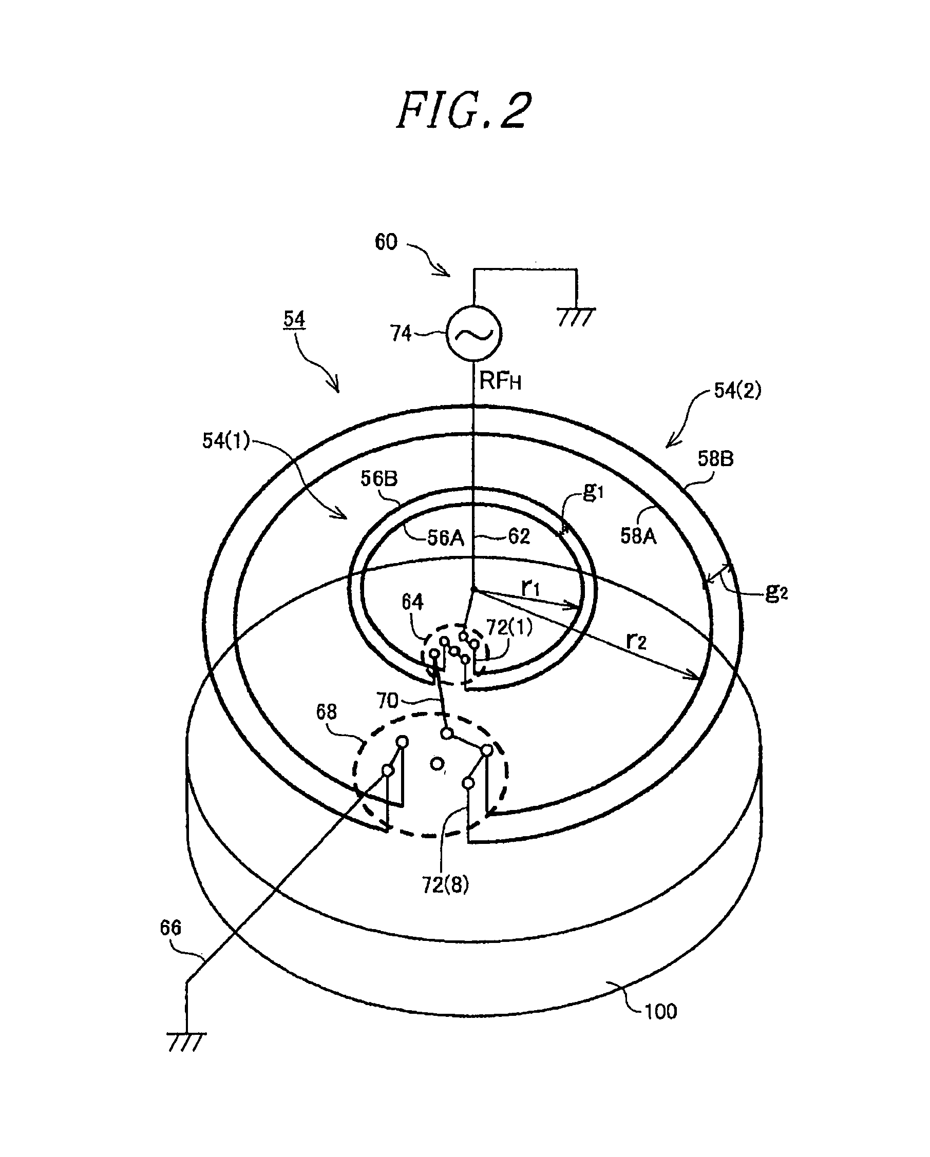
[0016]In the plasma processing apparatus in accordance with the first aspect of the present invention, when the parallel mode is selected, the high frequency branch currents flow through the first and the second coil segment in accordance with the distribution ratio depending on the impedances thereof in the same direction along the coil circling direction. Further, the electromotive force obtained by adding the branch currents flowing through a couple of coils contributes to the plasma generation in the processing chamber. When the multiplication series mode is selected, the high frequency current flows through the first and the second coil segment in the same direction along the coil circling direction, so that the electromotive force of the combination coil which contributes to the plasma generation in the processing chamber is doubled. When the minimization series mode is selected, the high frequency current flows through the first and the second coil segment in the opposite direction along the coil circling direction, so that the electromotive force is minimized. Therefore, even though the current actually flows through the couple of coils, the current hardly flows through the plasma in the processing chamber. By selectively switching the parallel mode, the multiplication series mode and the minimization series mode by the switching network, the current density distribution in the doughnut-shaped plasma generated in the processing chamber can be controlled near the position of the couple of coils (a pair of coil segments) in multiple steps.
[0018]In the plasma processing apparatus in accordance with the second aspect of the present invention, when the first parallel mode is selected, the high frequency branch currents flow through the first and the second coil segment in accordance with the distribution ratio of the impedances thereof in the same direction along the coil circling direction, and the electromotive force obtained by adding the branch currents flowing through the couple of coils contributes to the plasma generation in the processing chamber near the position of the combination coil (the first and the second coil segment). When the first multiplication series mode is selected, the high frequency current flows through the first and the second coil segment in the same direction along the coil circling direction, so that the electromotive force of the couple of coils which contributes to the plasma generation in the processing chamber is doubled near the position of the couple of coils. When the first minimization series mode is selected, the high frequency current flows through the first and the second coil segment in the opposite directions along the coil circling direction, so that the electromotive force is minimized. Therefore, even though the current actually flows through the couple of coils, the current hardly flows through the plasma in the processing chamber near the position of the couple of coils. By selectively switching the first parallel mode, the first multiplication series mode and the first minimization series mode by the switching network, the current density distribution in the doughnut-shaped plasma generated in the processing chamber can be controlled near the position of the couple of coils (a pair of coil segments) in multiple steps.
[0022]The basic configurations and operations of the plasma processing apparatus in accordance with the third aspect of the present invention are the same as those of the plasma processing apparatus in accordance with the first aspect of the present invention except in that each of the coil segments is divided in the coil circling direction. In terms of effects, although the configuration of the switching network becomes complicated, the wavelength effect can be reduced due to the short lengths of the coil segments. Further, the variation in the current density distribution in the same direction can be reduced due to the presence of a large number of terminals or open ends of the coil segments in the coil circling direction.
[0025]In accordance with the inductively coupled plasma processing apparatus and the plasma processing method therefor of the present invention, due to the above configuration and operation, loads of the RF power supply system are reduced, so that the uniformity or controllability of plasma density distribution can be improved with a simple structure of the RF antenna that can easily be manufactured.

Problems solved by technology

However, the uniformity of the plasma density on the substrate that is obtained by merely using a typical RF antenna is generally insufficient for the plasma process.

Method used


Image

  • Plasma processing apparatus and plasma processing method
  • Plasma processing apparatus and plasma processing method
  • Plasma processing apparatus and plasma processing method

Examples


Embodiment Construction

[0083]Hereinafter, embodiments of the present invention will be described with reference to the accompanying drawings which form a part hereof.

(Overall Configurations and Operations of Apparatus)

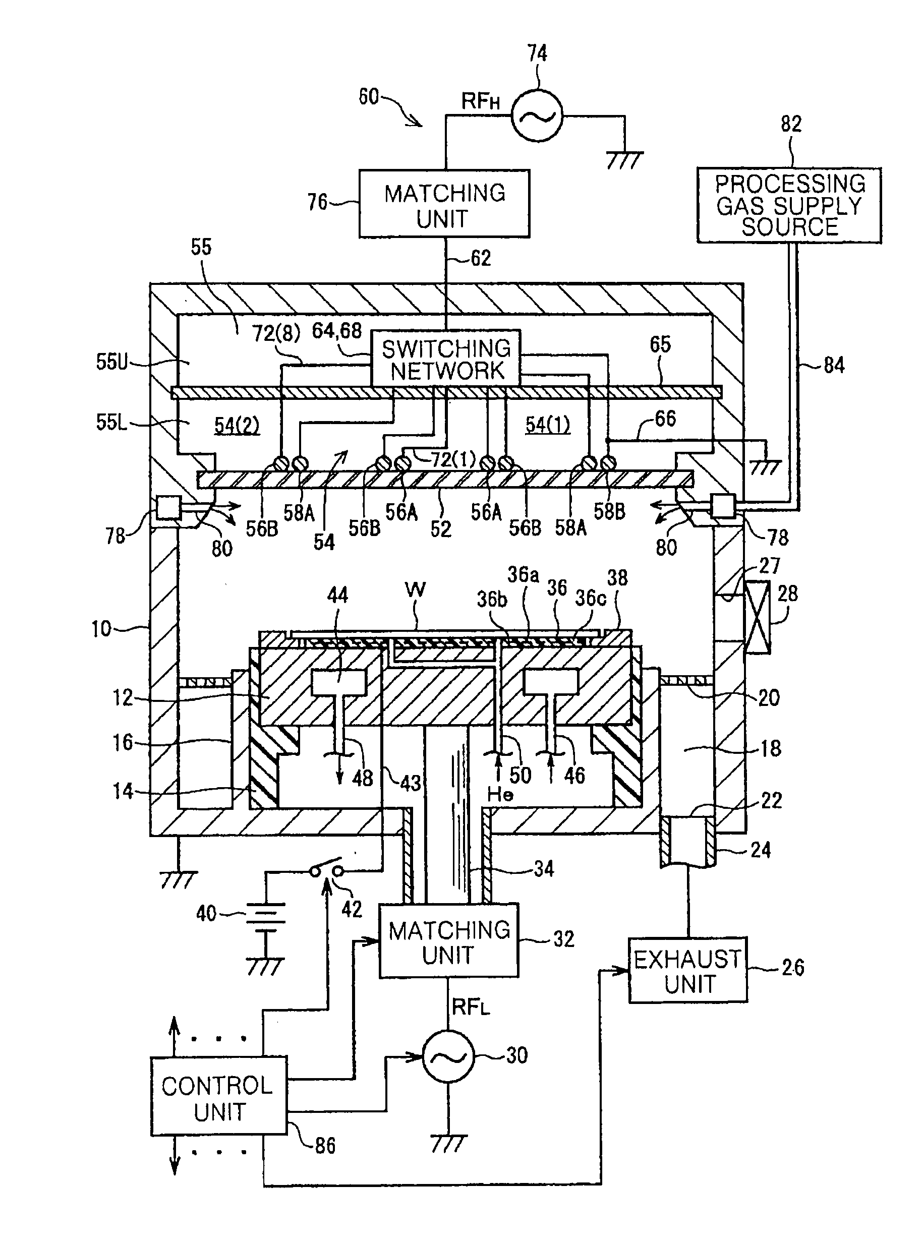
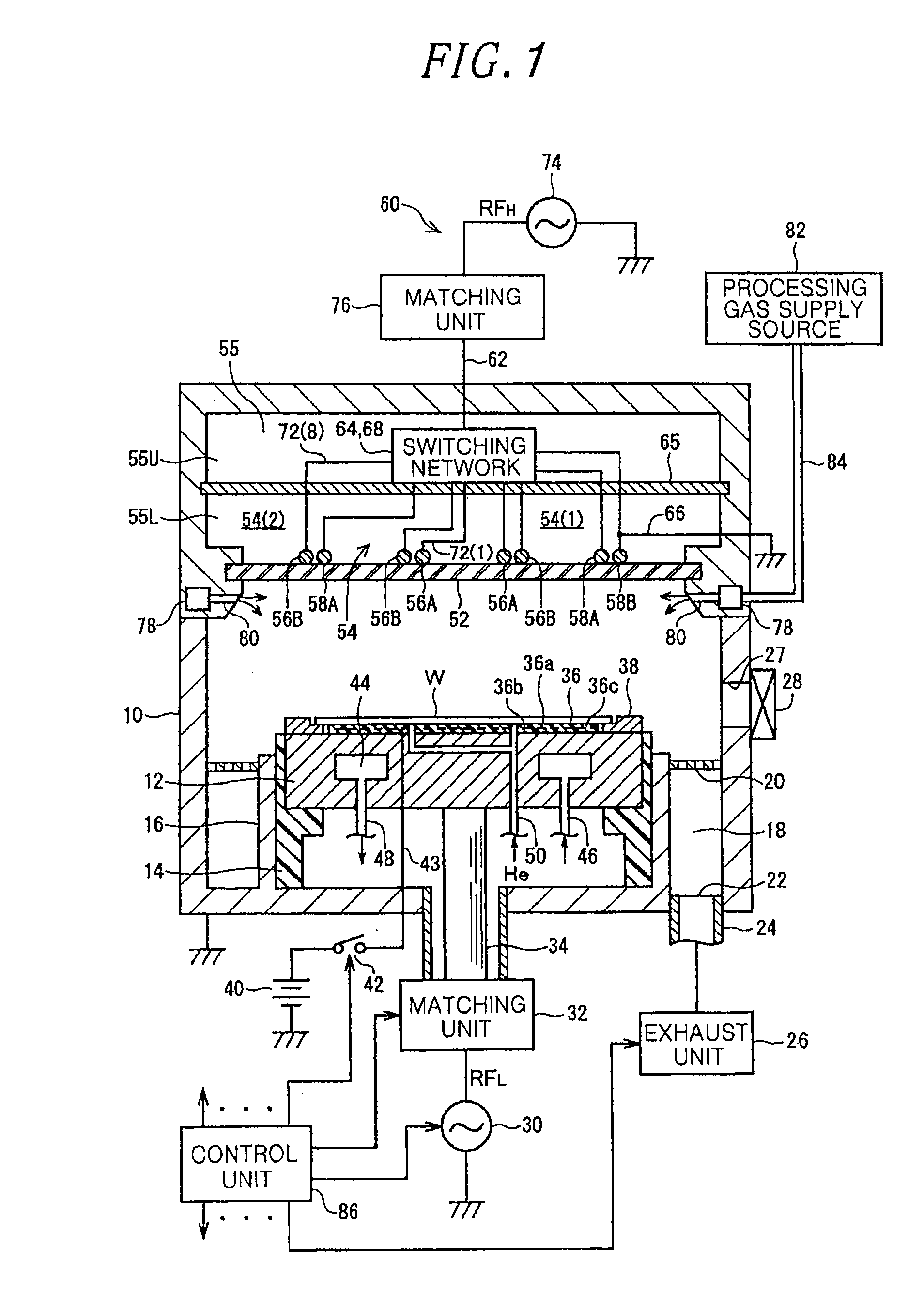
[0084]FIG. 1 shows a configuration of an inductively coupled plasma etching apparatus in accordance with an embodiment of the present invention. The inductively coupled plasma etching apparatus is of a type using a planar coil type RF antenna, and includes a cylindrical vacuum chamber (processing chamber) 10 made of a metal, e.g., aluminum, stainless steel or the like. The chamber 10 is frame-grounded.

[0085]In the inductively coupled plasma etching apparatus, various units having no involvement in plasma generation will be described first.

[0086]At a lower central portion of the chamber 10, a circular plate-shaped susceptor 12 for mounting thereon a target substrate, e.g., a semiconductor wafer W as a substrate supporting table is horizontally arranged. The susceptor 12 also serves as a high ...


PUM

PropertyMeasurementUnit
switching current distributionaaaaaaaaaa
capacitanceaaaaaaaaaa

Abstract

A plasma processing apparatus includes a vacuum evacuable processing chamber, at least a portion of which is formed of a dielectric window; a substrate supporting unit for supporting a target substrate in the processing chamber; and a processing gas supply unit for supplying a desired processing gas into the processing chamber. Further, the plasma processing apparatus includes an RF antenna provided outside the dielectric window; a high frequency power supply unit for supplying to the RF antenna a high frequency power; and a switching network switched among a parallel mode, a multiplication series mode, and a minimization series mode.

Description

FIELD OF THE INVENTION[0001]The present invention relates to a technique for performing a plasma process on a target substrate; and, more particularly, to an inductively coupled plasma processing apparatus and a plasma processing method therefor.BACKGROUND OF THE INVENTION[0002]In a manufacturing process of a semiconductor device or a flat panel display (FPD), a plasma is widely used in a process such as etching, deposition, oxidation, sputtering or the like since it has a good reactivity with a processing gas at a relatively low temperature. In such plasma process, the plasma is mostly generated by a high frequency discharge in the megahertz range. Specifically, the plasma generated by the high frequency discharge is classified into a capacitively coupled plasma and an inductively coupled plasma.[0003]Typically, an inductively coupled plasma processing apparatus includes a processing chamber, at least a portion of wall (e.g., a ceiling portion) of which is formed of a dielectric wi...

Claims


Application Information

Patent Timeline
Patent Type & Authority Applications(United States)
IPC IPC(8): H05H1/24C23C14/34C23C16/00
CPCH01J37/32174H01J37/321H01J37/32091H01L21/02315H01L21/0234H01L21/3065H01L21/32136H05H1/46
Inventor YAMAZAWA, YOHEI
Owner TOKYO ELECTRON LTD
Learn More