
Closed cell trench power mosfet structure and method to fabricate the same

Inactive Publication Date: 2011-09-22
SUPER GROUP SEMICON
View PDF1 Cites 9 Cited by
  • Summary
  • Abstract
  • Description
  • Claims
  • Application Information

AI Technical Summary

Benefits of technology

[0010]It is a main object of the present invention to reduce gate-to-drain capacitance of the closed cell trench power MOSFET structure by reducing junction area between the trenched gate and the drain region so as to enhance switching speed.
[0013]In contrast with the traditional closed cell trench MOSFET structure with a bottom of the trenched gate fully located in the drain region, in the closed cell trench MOSFET structure of the present invention, only the bottom of the stripe portion of the trenched gate is located in the drain region, and the bottom of the cross portion of the trenched gate is located in the body. Thus, the closed cell trench MOSFET structure is capable to effectively reduce junction area between the drain and the gate but maintain the channel width of the MOSFET structure. As a result, gate-to-drain capacitance of the closed cell trench MOSFET structure can be reduced with on-resistance being kept low.

Problems solved by technology

The feature of high gate-to-drain capacitance may restrict the switching speed of the transistor structure and hinder the development of high frequency electronic circuit applications.

Method used


Image

  • Closed cell trench power mosfet structure and method to fabricate the same
  • Closed cell trench power mosfet structure and method to fabricate the same
  • Closed cell trench power mosfet structure and method to fabricate the same

Examples


second embodiment

[0026]Moreover, in the present embodiment, the body 130 has a protruding area 130b on a lower surface thereof to have the bottom of the cross portion 172b of the trenched gate 172 located within the body 130. However, the present invention is not so restricted. FIGS. 3A and 3B show the closed cell trench MOSFET structure in accordance with the present invention, wherein FIG. 3B is a cross-section view corresponding to the cross-section C-C′ in FIG. 3A. In this embodiment, the lower surface of the body 230 is a flat plane, but the stripe portion 272a and the cross portion 272b of the trenched gate 272 are of different depth. The bottom of the stripe portion 272a is located below the lower surface of the body 230, but the bottom of the cross portion 272b is located above the lower surface of the body 230.

third embodiment

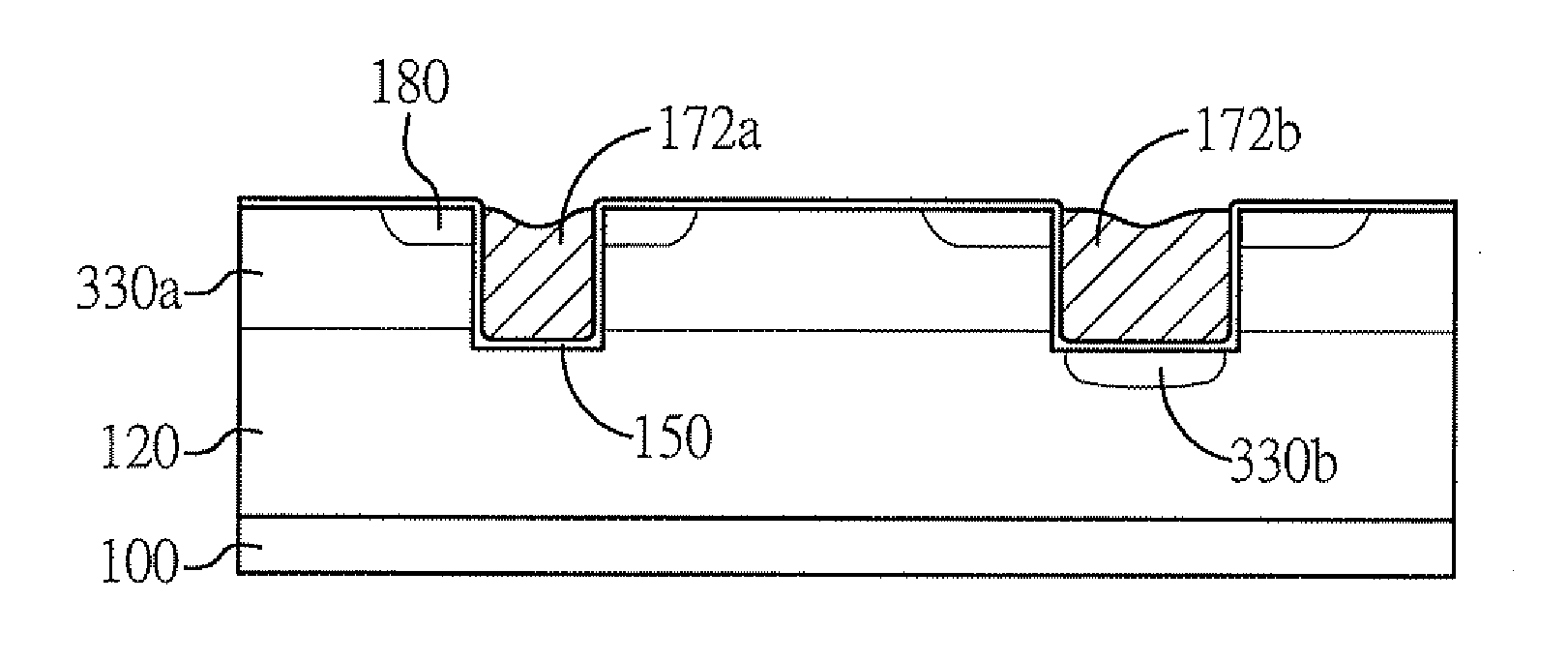
[0027]In the present embodiment, the body 130 has a downward protruding area 130b on a lower surface thereof to shield the bottom of the cross portion 172b of the trenched gate 172. But the present invention is not so restricted. As shown in FIG. 4, in accordance with the present invention, the body 330 can be separated into a first doped region 330a and at least a second doped region 330b. The second doped region 330b is located below the first doped region 330a and isolated from the first doped region 330a. The trenched gate 172 is located in the first doped region 330a. The bottom of the cross region 172b of the trenched gate 172 is located in the second doped region 330b.

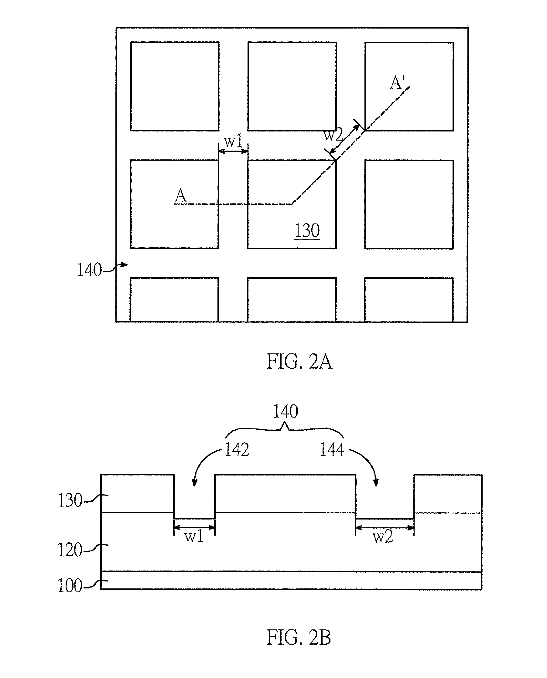
[0028]FIGS. 2A to 2J are schematic views showing a method to fabricate a closed cell trench MOSFET structure in accordance with a preferred embodiment of the present invention. FIG. 2B is a cross-section view respective to A-A′ cross section in FIG. 2A. Firstly, as shown in FIG. 2B, a substrate 100 of a first c...

fourth embodiment

[0033]It is worth noted that as shown in FIGS. 2A and 2B, the trench 140 in the present embodiment has longitude portions and traverse portions to define a plurality of square areas in the body 130. The source regions 180 are located in the square areas. The portion of the trench 140 at the intersection of the longitude portions and the traverse portions is defined as the cross region 144, and the rest of the trench 140 is defined as the striped regions 142. As shown in the top view of the semiconductor structure, the cross region 144 shows a square shape with a side length substantially identical to the width of the stripe region 142. However, the present invention is not so restricted. The cross region 144 may have an upper surface of different shapes according to the layout of the trench 140. Referring to FIG. 5, in the present invention, the trench 440 is sorted of three groups of different extending directions to define a plurality of triangles areas in the body 430. The source...


PUM


Abstract

A closed cell trench MOSFET structure having a drain region of a first conductivity type, a body of a second conductivity type, a trenched gate, and a plurality of source regions of the first conductivity type is provided. The body is located on the drain region. The trenched gate is located in the body and has at least two stripe portions and a cross portion. A bottom of the stripe portions is located in the drain region and a bottom of the cross portion is in the body. The source regions are located in the body and at least adjacent to the stripe region of the trenched gate.

Description

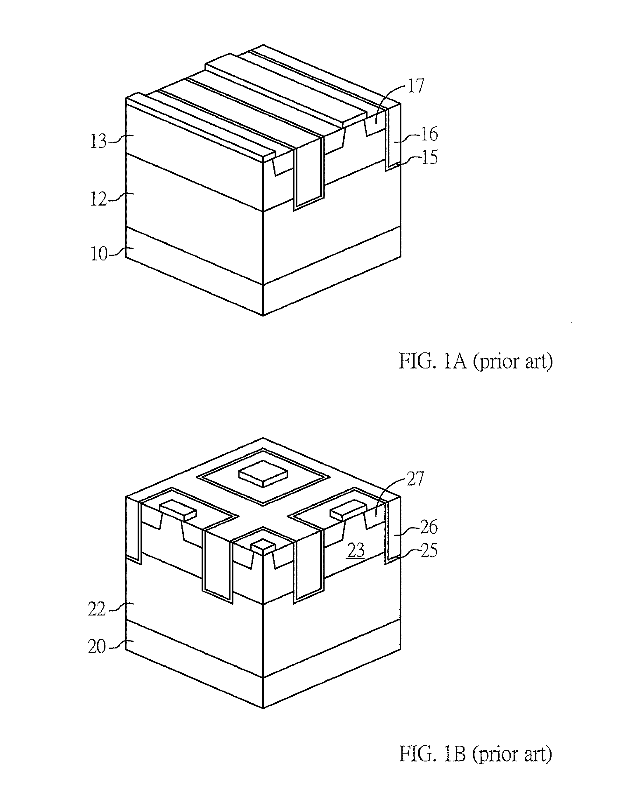
BACKGROUND OF THE INVENTION[0001]1. Field of the Invention[0002]This invention relates to a trench power metal oxide semiconductor field effect transistor (MOSFET) structure and a method to fabricate the same, and more particularly relates to a closed cell trench power MOSFET structure and a method to fabricate the same.[0003]2. Description of the Prior Art[0004]Attending with the developing of high frequency circuit applications, the demand of high switching speed transistors is increasing. The transistor structure with higher switching speed is capable to reduce switching loss so as to enhance power efficiency.[0005]FIG. 1A is a schematic view of a typical striped cell trench power MOSFET structure. As shown, the trench power MOSFET structure has an N-type heavily doped substrate 10, a N-type epitaxial layer 12, a P-type body 13, a gate oxide layer 15, a trenched gate 16, and a plurality of source regions 17. The epitaxial layer 12 is formed on the substrate 10. The body 13 is for...

Claims


Application Information

Patent Timeline
IPC IPC(8): H01L29/78H01L21/336
CPCH01L29/0623H01L29/0696H01L29/1095H01L29/7813H01L29/4238H01L29/66734H01L29/4236
Inventor HSU, HSIU WEN
Owner SUPER GROUP SEMICON
Learn More