Photo-curable composition having inherently excellent releasing property and pattern transfer property, method for transferring pattern usingthe composition and light recording medium having polymer pattern layer produced using the composition
a technology of releasing property and pattern transfer, applied in the field of photocurable composition, can solve the problems of disadvantage of existing photolithography methods, extended processing time, and inconvenient photolithography techniques, and achieve the effect of excellent releasing property
- Summary
- Abstract
- Description
- Claims
- Application Information
AI Technical Summary
Benefits of technology
Problems solved by technology
Method used
Image
Examples
example 1
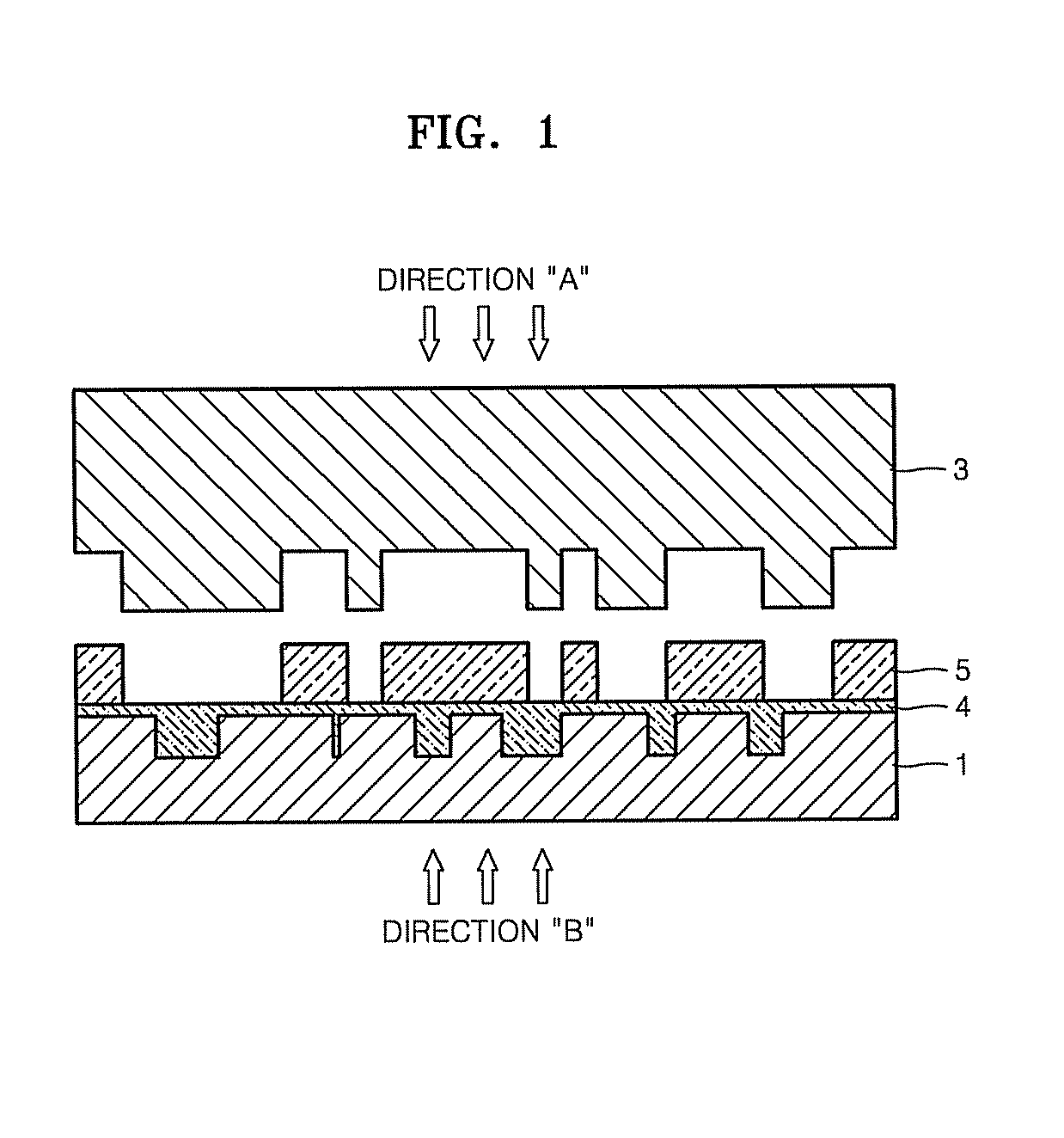
[0085]An optical disc was manufactured by transferring multi-layered patterns onto a substrate using a plastic stamper as a mold, prefabricated by a general method and using the photo-curable resin composition A. FIG. 2A is an atomic force microscope (AFM) view of the plastic stamper used in the current example. In FIG. 2A, bright portions indicate a plurality of convex parts for forming pit patterns on the substrate. FIG. 2B shows a pit depth profile of protrusion and non-protrusion patterns measured by scanning along the line “A” shown in FIG. 2A. In the stamper, an average pit depth scanned along the line “A” was 73.2 nm. The AFM view and pit depth profile were obtained using an Autoprobe M5 manufactured by Park Scientific Instrument.
[0086]An Ag—Pd—Cu (APC) alloy layer having an average thickness of about 30 nm was formed by a vacuum deposition process on an L0 recording layer having a predetermined pattern formed on a surface of a circular polycarbonate transparent substrate hav...
example 2
[0096]An optical disc was manufactured by transferring multi-layered patterns onto a substrate using a plastic stamper as a mold prefabricated by a general method and using the photo-curable resin composition B in the same manner as described in Example 1. FIG. 5A is an atomic force microscope (AFM) view of a plastic stamper used in the current example. In FIG. 5A, bright portions indicate a plurality of convex parts for forming pit patterns on the substrate. FIG. 5B shows a pit depth profile of protrusion and non-protrusion patterns measured by scanning along the line “A” shown in FIG. 5A. In the stamper, an average pit depth scanned along the line “A” was 73 nm. The AFM view and pit depth profile were obtained using an Autoprobe M5 manufactured by Park Scientific Instrument.
[0097]FIG. 6A is an AFM view of the polymer pattern layer formed on the substrate after performing the 50th imprinting on the photo-curable composition B using the same stamper. In FIG. 6A, dark portions indica...
example 3
[0099]An optical disc was manufactured by transferring multi-layered patterns onto a substrate using the plastic stamper used in Example 1 and using the photo-curable resin composition C in the same manner as described in Example 1.
[0100]Even after performing the 50th imprinting, no contamination was observed from the stamper. Further, appreciable deformation of the polymer pattern layer was not observed while performing the imprinting 50 times.
[0101]With regard to jitter values, measurements after performing the first and the 50th imprintings were both 7.9%, as measured by the same tester used in Example 1. As to the tilt characteristic in case of recording using a five-layered optical disc, substantially the same evaluation result as in Example 1 was obtained.
PUM
| Property | Measurement | Unit |
|---|---|---|
| height | aaaaa | aaaaa |
| width | aaaaa | aaaaa |
| temperature | aaaaa | aaaaa |
Abstract
Description
Claims
Application Information
 - R&D
- Intellectual Property
- Life Sciences
- Materials
- Tech Scout
- Unparalleled Data Quality
- Higher Quality Content
- 60% Fewer Hallucinations
Browse by: Latest US Patents, China's latest patents, Technical Efficacy Thesaurus, Application Domain, Technology Topic, Popular Technical Reports.
© 2025 PatSnap. All rights reserved.Legal|Privacy policy|Modern Slavery Act Transparency Statement|Sitemap|About US| Contact US: help@patsnap.com


