Mosfet with gate pull-down

a mosfet and gate pull-down technology, applied in the field of mosfet, can solve the problems of limited by the switching losses of the power switch, the switching loss, and the impairment of the system reliability, and achieve the effect of reducing or preventing the conductance of the low-side mosfet switch during turn-off and reducing the switching loss

Inactive Publication Date: 2011-06-23
TEXAS INSTR INC
View PDF33 Cites 55 Cited by
  • Summary
  • Abstract
  • Description
  • Claims
  • Application Information

AI Technical Summary

Benefits of technology

Another aspect of the invention is provided by a method of operating a switching DC to DC converter comprising alternately turning on and off a high-side MOSFET switch and a low-side switch. When turning the low-side MOSFET switch off, utilizing the Miller effect voltage on a gate of a pull-down MOSFET to operate the pull-down MOSFET to couple a gate of the low-side MOSFET switch to a source thereof, whereby conduction in the low-side MOSFET switch during turn-off is reduced or prevented.
Yet another aspect of the invention includes a high-side switch with a main power MOSFET incorporating a pull-down FET. A pull-down MOSET has a drain connected to the gate of the main power MOSFET and a source connected to the source of the main power MOSFET. A gate of the pull-down MOSFET is connected to one terminal of a capacitor, another terminal of the capacitor is connected to the drain of the main power MOSFET, whereby dv / dt of a signal at the drain of the main power MOSFET during turn-off of the main power MOSFET causes the pull-down MOSFET to turn-on via capacitive coupling and speed-up the turn-off of the main power MOSFET. The hard turn-off of the high-side switch reduces the switching losses associated with this transistor.

Problems solved by technology

In an article entitled “The future of Discrete Power in VRM Solutions,” at the Intel Technology Symposium 2003, Jon Hancock describes the advantages that can be achieved by increasing the switching frequency, but this is limited by the switching losses of the power switches.
One source of switching losses is the shoot-through current that occurs when the low-side switch is turned back on during the conduction period of the high-side switch which is caused by bouncing of the gate electrode bias of the low-side switch.
This effect has to be avoided as it leads to significant power loss, and if repetitive, will impair the reliability of the system.
One solution is to utilize transistors that have a higher Vth, but such transistors usually have a higher Rds,on which leads to higher conduction losses.
At the end of the delay time, the diode is commutated by the changing polarity of the voltage at the switch node and the associated reverse recovery current peak adds to the nominal current increasing switching power loss.
Any power loss decreases the efficiency of the power conversion and high switching loss inhibits the aimed increase in the switching frequency.
This, of course, reduces the switching efficiency of the high-side switch.
However, this exacerbates the shoot-through problem as discussed above.

Method used


Image

  • Mosfet with gate pull-down
  • Mosfet with gate pull-down
  • Mosfet with gate pull-down

Examples


Embodiment Construction

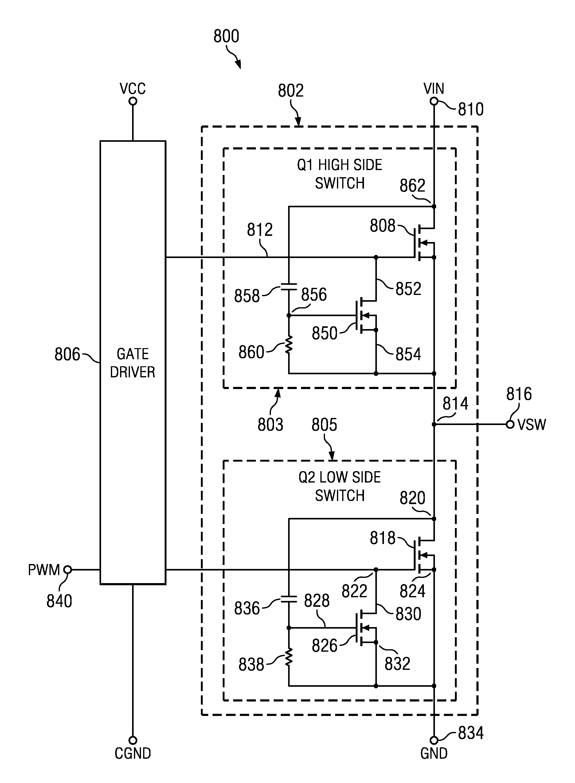
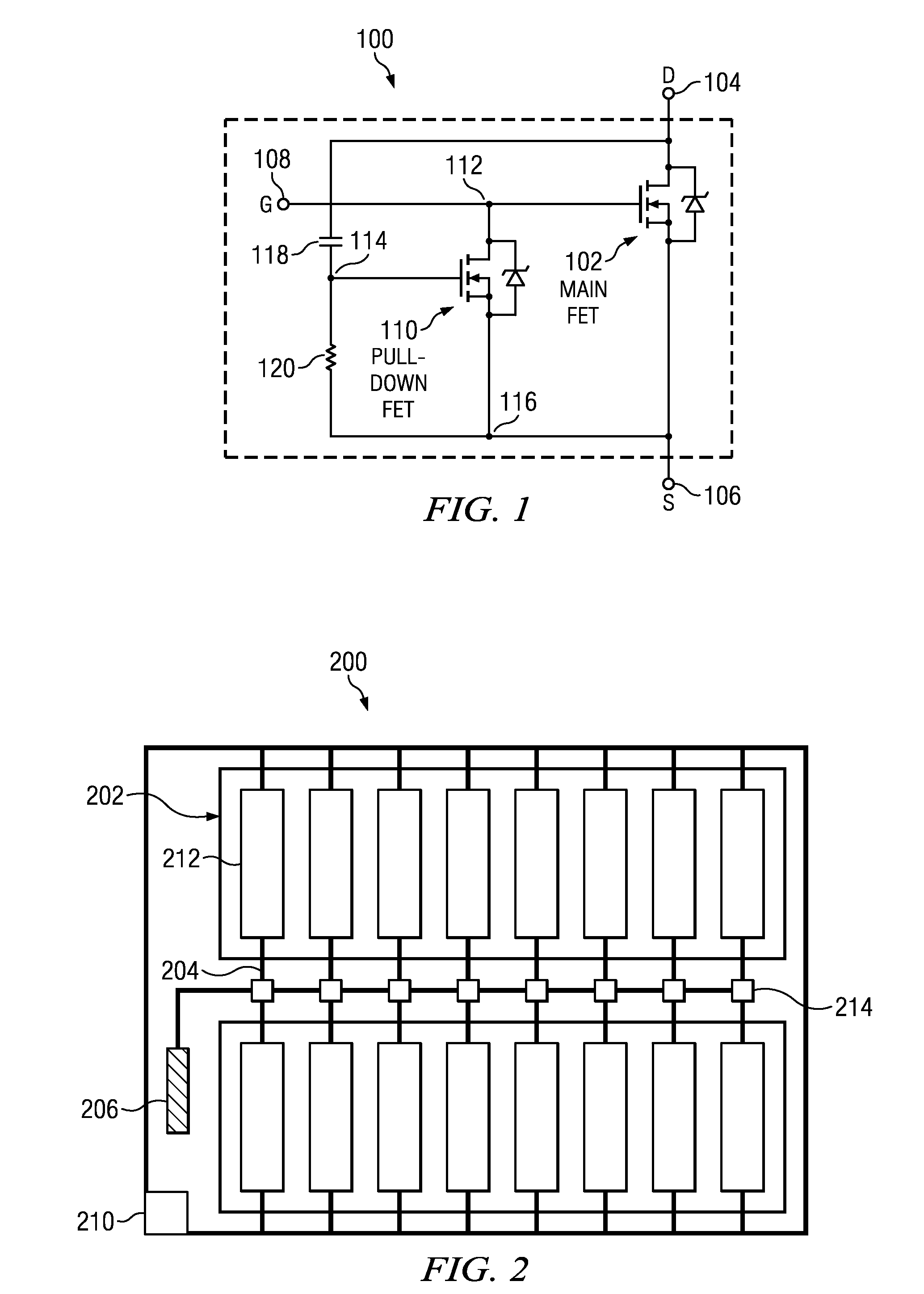
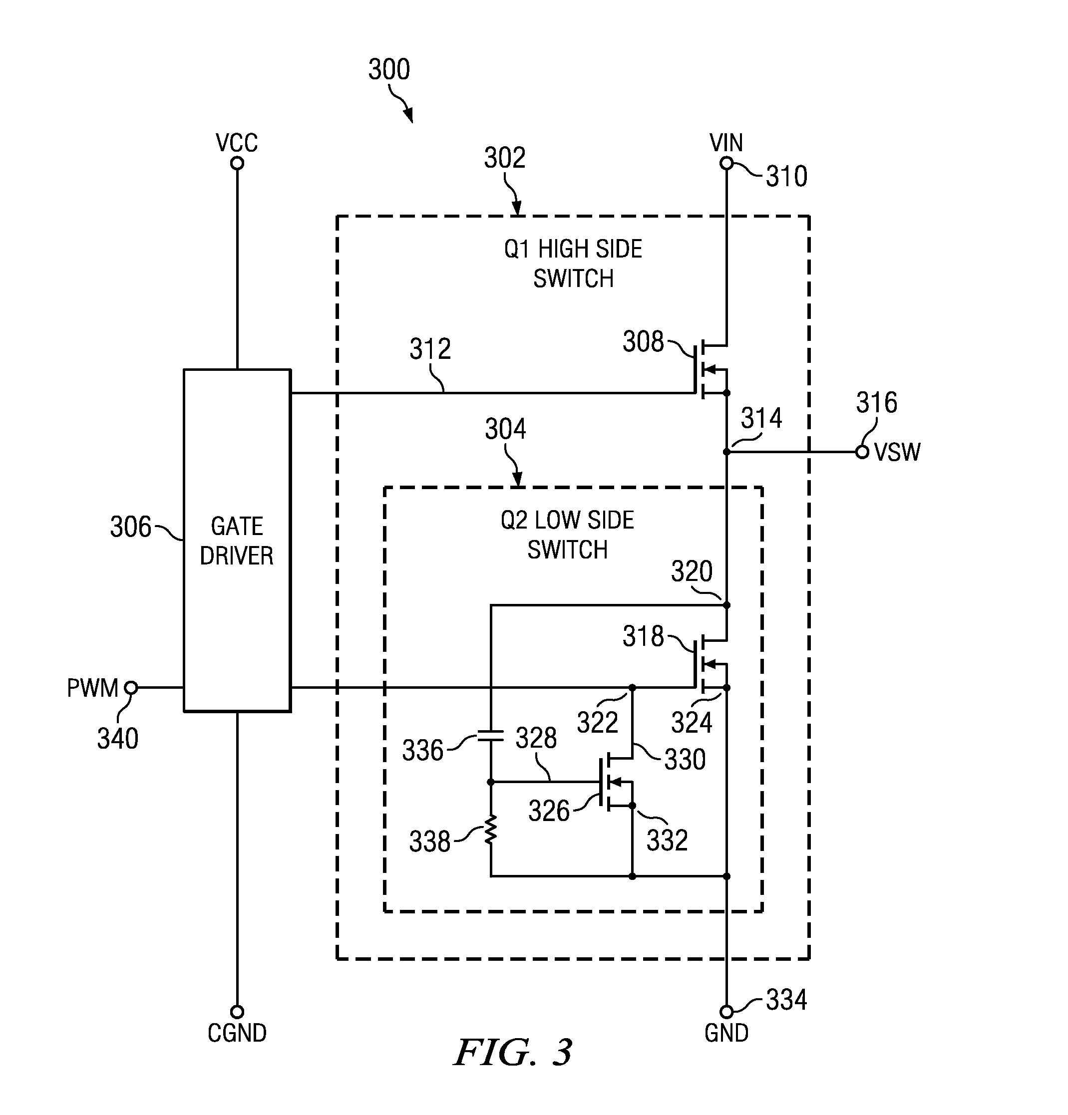
An embodiment of the present invention is shown in FIG. 1, generally as 100. Although this embodiment as shown and discussed is for a low-side switch for a synchronous buck converter, the invention is not so limited, and an embodiment in which the invention is utilized in both the low-side and high-side switches will be discussed later in connection with FIG. 8. As easily recognized by people skilled in the art, the embodiment shown in FIG. 1, can be implemented at any switching power MOSFET, and especially can be implemented at MOSFETs used in push-pull configuration in any switched DC / DC converter topology. Also, the solution using a capacitive coupling to turn-on the pull-down transistor can be implemented in lateral power MOSFETs used in IC's designed for power management applications.

As shown in FIG. 1, the main FET, which as shown, is a NMOS transistor, has a drain 104, a source 106 and a gate 108. A second FET, the pull-down FET 110, is connected so that its drain is connecte...


PUM


Abstract

A MOSFET main switch transistor has a pull-down FET coupled between a drain thereof and the gate of the main switch transistor. A gate of the pull-down FET is coupled to the drain of the main switch transistor by a capacitor and is connected to a source thereof by a resistor. The pull-down FET is operated by capacitive coupling to the voltage drop across the main switch and can be used to hold the gate of the main switch transistor at or near its source potential to avoid or reduce unintentional turn-on of the main switch transistor by the Miller effect.

Description

FIELD OF THE INVENTIONThe present invention relates to a MOSFET in which bouncing of the gate bias leading to unintentional turn-on of the device is limited or eliminated, and in particular to such a device in a push-pull stage of a converter operating in a switching mode.BACKGROUND OF THE INVENTIONSwitching mode DC to DC converters are commonly used to provide conversion from one DC voltage to another at high efficiency. Improving the efficiency of such converters is an important design goal, especially where large banks of such converters are operating within the same space, such as in computer server farms. In these situations, the improvement in the efficiency of the converter not only reduces the amount of power the converter consumes, but dramatically reduces the cooling load placed upon the premises.Methods to improve the efficiency of switching type DC to DC converters have been extensively studied. In an article entitled “The future of Discrete Power in VRM Solutions,” at t...

Claims


Application Information

Patent Timeline
Patent Type & Authority Applications(United States)
IPC IPC(8): G05F1/00H03K17/687
CPCH03K17/687H03K17/165
Inventor XU, SHUMINGKOREC, JACEKLOPEZ, OSVALDO J.
Owner TEXAS INSTR INC
Why Eureka
Try Eureka