Thin-film capacitor and manufacturing method thereof

Active Publication Date: 2011-03-31
TDK CORPARATION
View PDF13 Cites 15 Cited by
  • Summary
  • Abstract
  • Description
  • Claims
  • Application Information

AI Technical Summary

Benefits of technology

[0007]The present invention has been made in light of the above-described problems. It is an object of the present invention to provide a thin-film capacitor capable of improving the stability of electric connection between an internal electrode layer and a connection electrode and a method of manufacturing the thin-film capacitor.
[0010]According to such a thin-film capacitor and a method of manufacturing the thin-film capacitor, the internal electrode layer is connected to the connection electrode via at least a part of the surface and the end face of the internal electrode layer included in the projecting portion of the internal electrode layer, and therefore the contact area between the both can be increased and the connection state can be stabilized. Furthermore, because the projection portion is formed so that the ratio L / t between the projection amount L of the projecting portion of the internal electrode layer with respect to the dielectric layer and the thickness t of the internal electrode layer becomes 0.5 to 120, the projection amount of the projecting portion can be within an appropriate range suitable to be able to connect the projecting portion and the connection electrode, and the connection state between the internal electrode layer and the connection electrode can be stabilized further. As a result, the stability of electric connection between the internal electrode layer and the connection electrode can be improved. Then, once the stability of the connection state is improved, the production yield will increase and the reliability will also improve.
[0011]Moreover, the method preferably includes the step of exposing the end face of the internal electrode layer after the step of forming the laminated body and prior to the step of wet etching. Thus, the amount of erosion of the dielectric layer by the wet etching treatment is fixed, and therefore the projection amount of the projecting portion of the internal electrode layer can be fixed, thereby suppressing the variations in performances of the thin-film capacitor and further improving the reliability.
[0012]The thin-film capacitor and the manufacturing method thereof according to the present invention can improve the stability of electric connection between the internal electrode layer and the connection electrode.

Problems solved by technology

However, in attempting to apply the configuration of the laminated ceramic capacitor described in Patent Document 1 to a thin-film capacitor in order to achieve a large capacity thin-film capacitor, the following problems may arise.
However, with these methods, only an end face portion of the internal electrode having a very thin film-thickness is exposed and the connection to the connection electrode is made only with this end face portion, and therefore the connection state between the internal electrode layer and the connection electrode is likely to be unstable.
This connection instability results in a decrease in the production yield or a decrease in the reliability.

Method used


Image

  • Thin-film capacitor and manufacturing method thereof
  • Thin-film capacitor and manufacturing method thereof
  • Thin-film capacitor and manufacturing method thereof

Examples


example 1

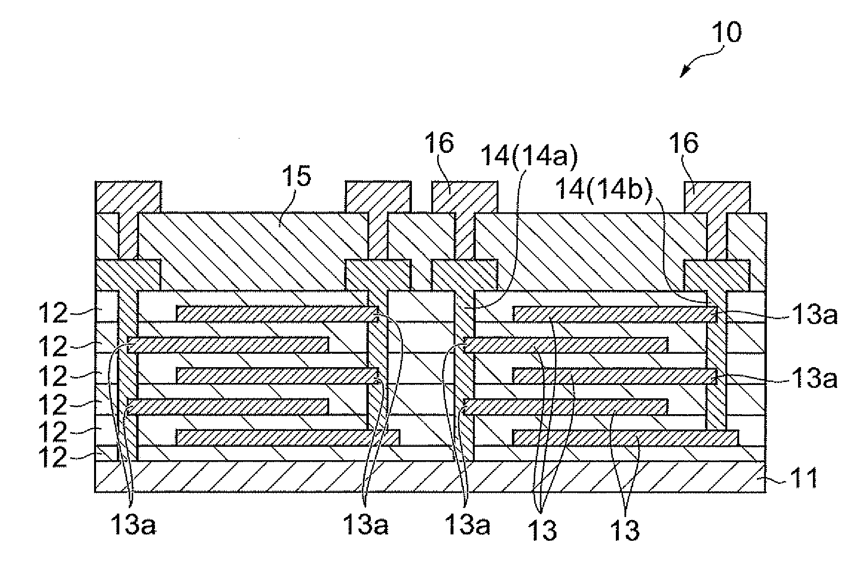
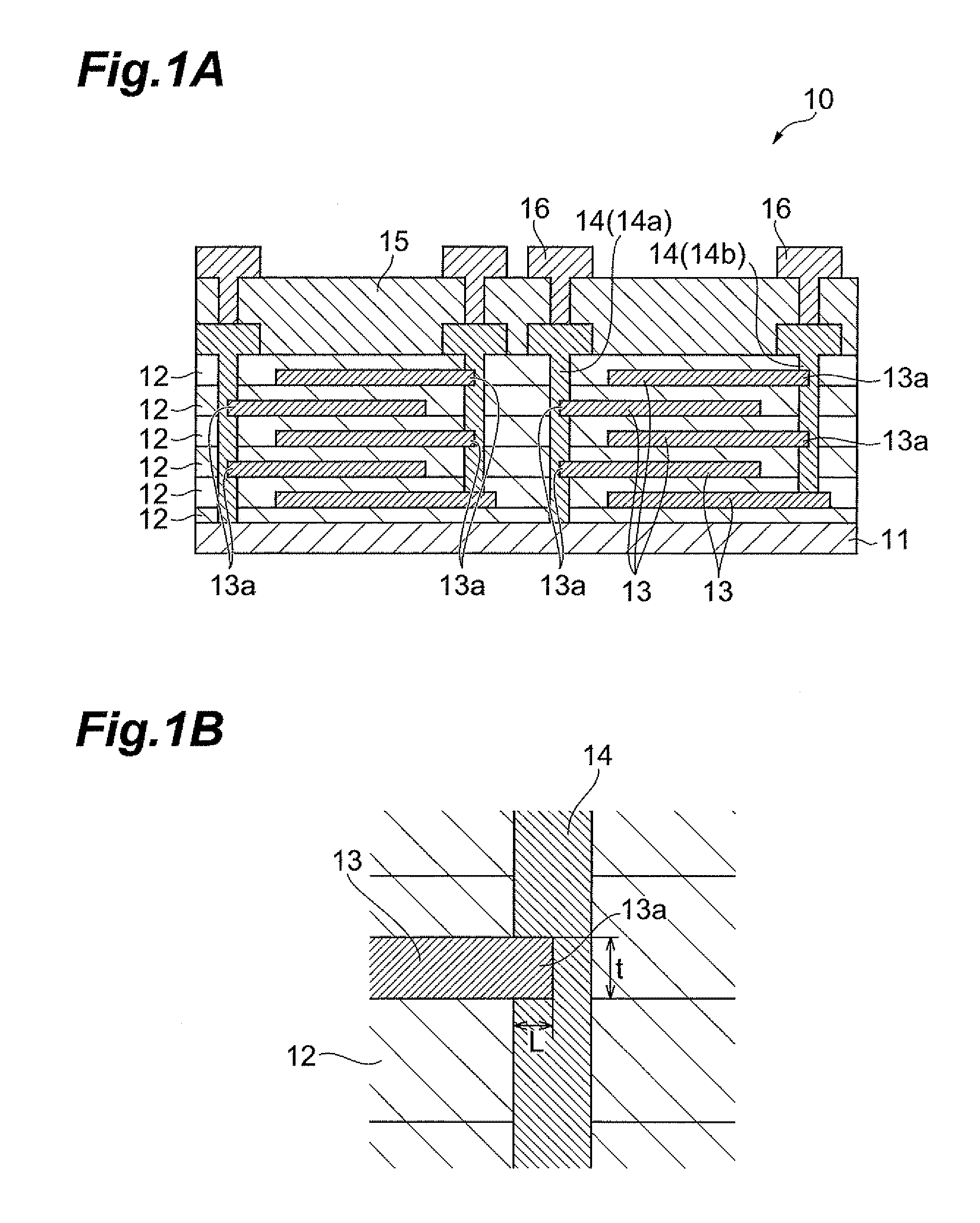
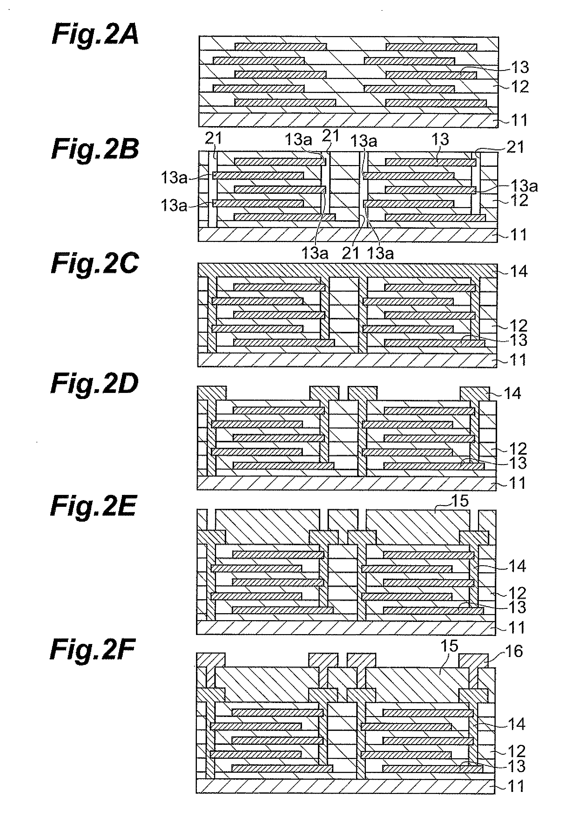
[0036]Above the base electrode 11 made of Ni foil, the dielectric layer 12 and the patterned internal electrode layer 13 were alternately deposited by sputtering or the like. Eleven dielectric layers 12 were deposited. Thus, the number of the dielectric layers 12 sandwiched by the Ni substrate 11 and the internal electrode layers 13 is ten. The electrode geometry and the dielectric thickness were set so that one dielectric layer 12 may produce about 10500 pF (10.5 nF).

[0037]After depositing the dielectric layers 12 and the internal electrode layers 13, a resist layer was formed which has the opening 21 at a position, where connection to the internal electrode can be made, on the heat-treated assembly. Subsequently, the dielectrics 12 of the opening 21 was etched with an etchant. At this time, an etchant which etches the dielectric layer 12 but does not etch the internal electrode layer 13 was selected. Specifically, as described above, if the dielectric film 12 is made of BT, BST, o...

example 2

[0039]As with Example 1, the dielectric layers 12 and the internal electrode layers 13 were deposited, and furthermore a resist layer provided with the opening 21 was formed, and subsequently the opening 21 was removed by ion milling. Subsequently, the dielectric side wall of the opening 21 was etched with an etchant. As with Example 1, the capacitances of the capacitors were measured and the average value and standard deviation thereof were calculated.

example 3

[0040]A laminated body similar to that of Example 1 was prepared, and a slit was formed at a place located in the opening 21 for connecting the internal electrode layer 13 by dicing or the like. Subsequently, the dielectric of the end face portion of the internal electrode layer 13 was etched with a dielectric etchant. As with Example 1, the capacitances of the capacitors were measured and the average value and standard deviation thereof were calculated.


PUM

PropertyMeasurementUnit
Capacitanceaaaaaaaaaa

Abstract

To provide a thin-film capacitor capable of improving the stability of electric connection between an internal electrode layer and a connection electrode. The thin-film capacitor comprises: two or more dielectric layers deposited above a base electrode; an internal electrode layer being deposited between the dielectric layers and having a projecting portion which projects from the dielectric layer when seen from a laminating direction; and a connection electrode electrically connected to the internal electrode layer via at least a part of a surface and an end face of the internal electrode layer included in the projecting portion, wherein a ratio L / t between a projection amount L of the projecting portion of the internal electrode layer with respect to the dielectric layer and a thickness t of the internal electrode layer is 0.5 to 120.

Description

BACKGROUND OF THE INVENTION[0001]1. Field of the Invention[0002]The present invention relates to thin-film capacitors and manufacturing methods thereof.[0003]2. Related Background of the Invention[0004]As with a laminated ceramic capacitor, for example, described in Patent Document 1 (Japanese Patent Application Laid-Open No. 2009-155118), a configuration is known wherein a dielectric layer and an internal electrode layer are alternately deposited to form a multilayer laminated body and wherein on both ends of this laminated body the internal electrode layer is connected to an external electrode.SUMMARY OF THE INVENTION[0005]However, in attempting to apply the configuration of the laminated ceramic capacitor described in Patent Document 1 to a thin-film capacitor in order to achieve a large capacity thin-film capacitor, the following problems may arise. In the case of the thin-film capacitor, an internal electrode layer is exposed on a side face of a dielectric layer with the use of...

Claims


Application Information

Patent Timeline
IPC IPC(8): H01G4/005H01G9/00
CPCH01G4/33Y10T29/417H01G4/005
Inventor OIKAWA, YASUNOBUYANO, YOSHIHIKO
Owner TDK CORPARATION
Why Eureka
Try Eureka