
Arrangement for solder bump formation on wafers

a technology of solder bumps and wafers, applied in the direction of soldering apparatus, semiconductor/solid-state device details, manufacturing tools, etc., can solve the problems of complex process, achieve void free production of solder bumps, reduce costs, and reduce costs

Active Publication Date: 2011-03-03
SEMLGEAR INC
View PDF3 Cites 2 Cited by
  • Summary
  • Abstract
  • Description
  • Claims
  • Application Information

AI Technical Summary

Benefits of technology

[0014]In a further embodiment of the present apparatus, the first or lower compression plate may have a slightly convex or cylindrically shaped uppermost surface thereon and the second or upper plate may have a corresponding cylindrically or a somewhat convex shaped surface thereon so as to provide a rollable or rockable “squeegee” effect to a pattern plate supportably compressed therebetween. Such a curved upper plate and correspondingly curved lower support plate could be articulated side-to-side to provide a squeezing and excess solder-removal action to a pattern plate with its associated through-holes with temporarily molten solder. Such excess solder removal would thus shorten the manufacturing process by combining several steps into one operation of filling those through-hole and cleaning the surface of the pattern plate almost simultaneously.
[0019]Alignment of a patterned plate and a wafer or substrate in the prior art is often an operation which consumes time and expense. One such apparatus for minimizing the expense, the time and the possible inaccuracies associated therewith, would be to present an apparatus for supporting the patterned plate in a hinged-correspondence to a plate for supporting the wafer. Moving the support for the patterned plate and the wafer via a hinged support arrangement, to provide automatic and prompt alignment therebetween preceding a heating and chilling operation therewith for the deposition of those solder bumps onto that wafer is presented herewith.
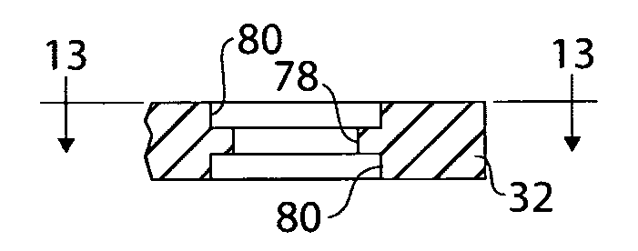
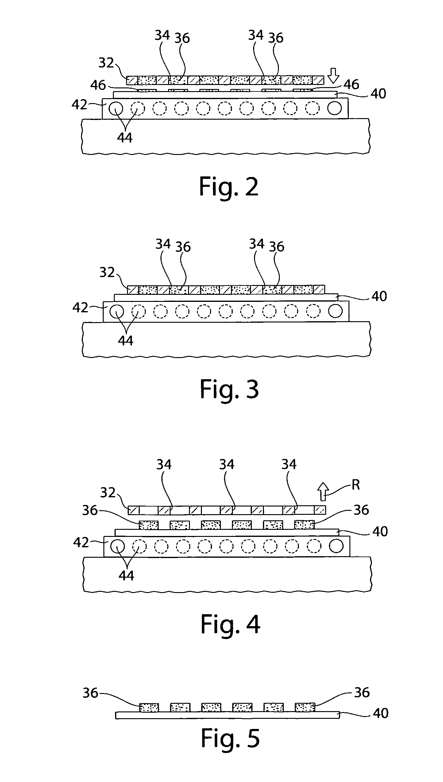
[0020]The invention thus comprises a process for the manufacture of a wafer substrate for use in the semiconductor industry, comprising one or more of the following steps: arranging a first compressive member and a second compressive member in an opposed, compressibly displacable, spaced-apart relationship, with a pattern plate disposed therebetween, the pattern plate having a plurality of aligned through-holes arranged thereon; filling the through-holes with a molten solder; compressing the solder and the pattern plate between the first and the second opposed compressive members to compact the solder therein and cleans the pattern plate of excess solder; chilling the pattern plate to solidify the molten solder in the through-holes; and removing the pattern plate from the spaced-apart compressive members. The process may include placing the pattern plate on the wafer substrate in an aligned manner; heating the solder in the through-holes in the pattern plate to as to melt and cause adherence of the solder to the wafer as solder bumps thereon. The first compressive member and the second compressive member may have correspondingly curved facing surfaces to effect an excess solder removal operation during compression of the pattern plate therebetween. The compressive members may be plates. The curved facing surfaces of the compressive members may be of convex shape. The curved facing surfaces of the compressive members may be of slightly cylindrical shape. The compressing of the pattern plate may occur in a generally vertical orientation. The compressive members may be comprised of rotatable rollers. The through-holes may be straight bores arranged through the pattern plate. The through-holes may be openings having a hemispherical depression on one side of the plate in communication with a bore from the side of the pattern plate. The through-holes may be openings through the pattern plate having a pinched waist portion. The bores may have a slot arranged thereacross to define a keyway on at least one side of the pattern plate. The first compressive member and the second compressive member may be hinged together on a hinge pair member arrangement to provide pre-aligned mating of the pattern plate and the wafer / substrate. The compressive members may be supported by an articulable support to move the compressive members side to side with respect to one another and the pattern plate pinched therebetween. The process may include pivoting the pattern plate into mating alignment with the wafer / substrate for initiation of transfer of solder from the pattern plate to the wafer / substrate. The process may include applying an energy field to said pattern plate to facilitate void free production of solder bumps in said pattern plate.

Problems solved by technology

Such production methods to date, are very involved, utilizing complicated automatic manufacturing techniques.
This particular prior art shows a plurality of steps for applying a solder to a substrate, utilizing a variety of steps including alignment plates and associated procedures therewith which makes the process somewhat complicated.

Method used


Image

  • Arrangement for solder bump formation on wafers
  • Arrangement for solder bump formation on wafers
  • Arrangement for solder bump formation on wafers

Examples


Embodiment Construction

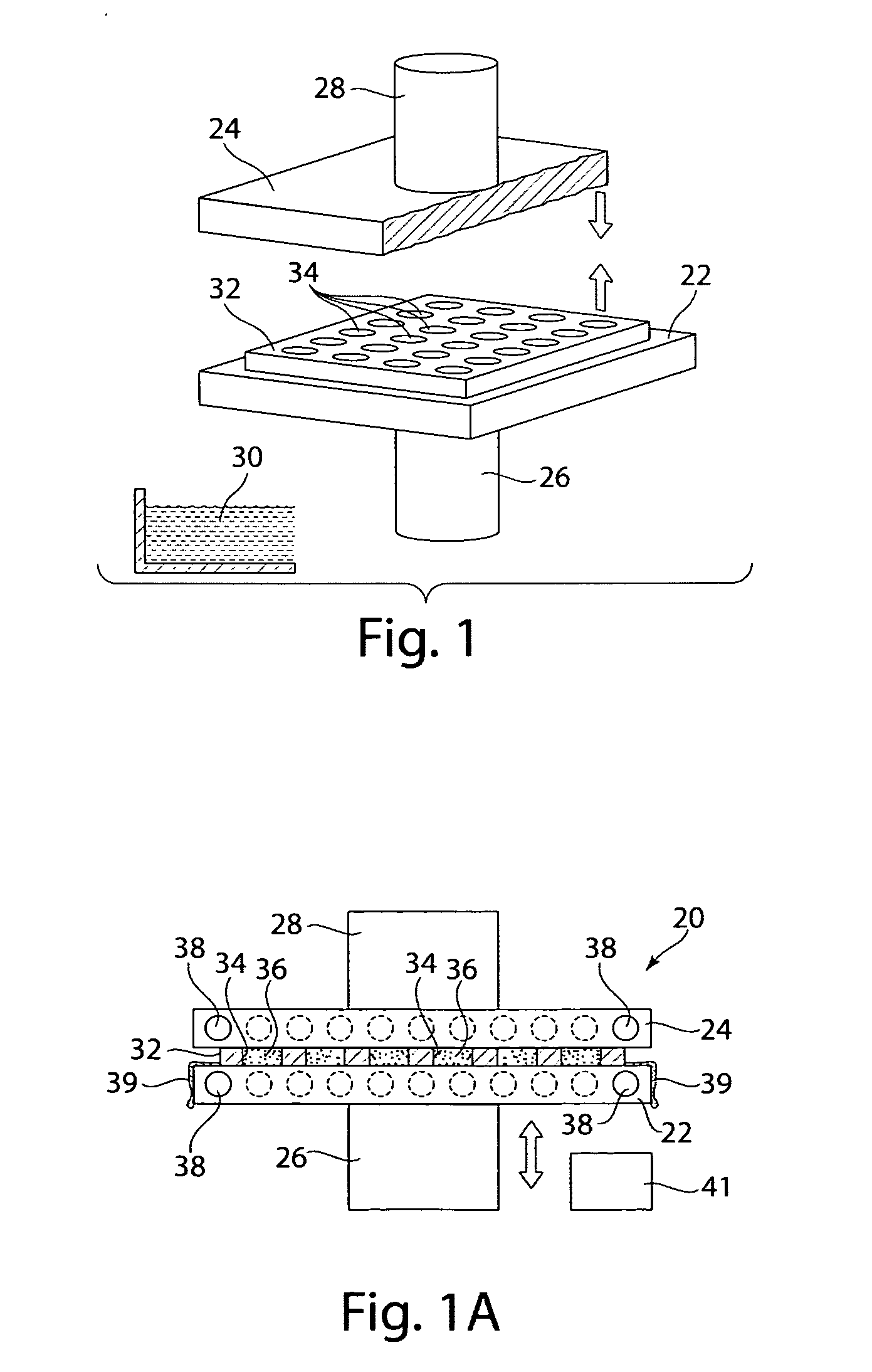
[0038]Referring now to the drawings in detail, and particularly to FIG. 1, there is shown the present invention, which comprises a method and apparatus for generating, depositing and forming an accurate array of solder bumps on a substrate such as a wafer of for example silicon, or on a layer of plate glass. These solder bumps are utilized to form an array of electrical contacts on that substrate, wafer of plate, for use in the electronics industry.

[0039]The initial apparatus of the present invention, represented in FIG. 1 thus comprises a solder-loading assembly 20 consisting of a first or lower support compression plate 22 and a second or upper compression plate 24 (only partially shown, for clarity). The first or lower support plate 22 of the assembly 20 may be movably supported on lower plate drive 26 and the second or upper plate 24 may be supported by an upper plate drive 28, wherein each drive 26 and 28 may be movable for compressably advancing the lower and upper plates 22 a...


PUM


Abstract

An apparatus and a process for the manufacture of a solder-bump adhered wafer substrate for use in the semiconductor industry, comprising one or more of the following steps including: arranging a first compressive member and a second compressive member in an opposed, compressibly displaceable, spaced-apart relationship, with a pattern plate disposed therebetween with the pattern plate having a plurality of aligned through-holes arranged thereon; filling the through-holes with a molten solder; compressing the solder and the pattern plate between the first and second opposed compressive members to compact the solder therein and cleans the pattern plate of excess solder; chilling the pattern plate to solidify the molten solder in the through-holes; and removing the pattern plate from the spaced-apart compressive members to produce a wafer with solder bumps thereon.

Description

BACKGROUND OF THE INVENTION[0001]1. Field of the Invention[0002]The present invention relates to method and apparatus for forming solder bumps on substrates such as silicon wafers for utilization in chip manufacturing in the electronics industry.[0003]2. Prior Art[0004]The manufacturer of integrated circuits in the production of semiconductor devices is an evolving field. Their high demand in commerce has required greater speed in their manufacture and further necessitates improvements in environmental control during their manufacture[0005]The current manufacturer of such semiconductor devices is initially accomplished by the deposition of solder at discreet points on a silicon wafer or base carrier. Such production methods to date, are very involved, utilizing complicated automatic manufacturing techniques. For example, U.S. Pat. No. 6,832,747 to Cordes et al, shows a process for utilizing hybrid molds for a molten solder screening process. This process developed a pyramidal shaped...

Claims


Application Information

Patent Timeline
Patent Type & Authority Applications(United States)
IPC IPC(8): H01L21/60B22D27/11
CPCB23K3/0623B23K2201/40H01L24/11H01L24/742H01L2224/13099H01L2224/11334H01L2924/01013H01L2924/14H01L2924/014H01L2224/1131H01L2924/01005B23K2101/40H01L2924/15788H01L2924/00014H01L2924/00011H01L2924/00H01L2224/0401
Inventor LEE, CHUNGHSINZHANG, JIAN
Owner SEMLGEAR INC
Learn More