Active device array mother substrate and method of fabricating display panel

a technology of active devices and mother substrates, which is applied in the direction of electrical devices, semiconductor devices, instruments, etc., can solve the problems of reduced display contrast ratio of lcd, easy to affect curing lines, and limited aperture ratio of display

Active Publication Date: 2011-03-03
AU OPTRONICS CORP
View PDF4 Cites 11 Cited by
  • Summary
  • Abstract
  • Description
  • Claims
  • Application Information

AI Technical Summary

Benefits of technology

[0011]The invention is directed to a method of fabricating a display panel. The method prevents curing lines from being affected by a doping process of pixel arrays, thereby solving issues such as peeling of the curing lines of a PSA curing circuit in the fabrication process.
[0022]In light of the foregoing, the curing lines are formed in the same layer as the source conductor and the drain conductor of the active devices in the active device array mother substrate of the invention. Therefore, the curing lines are prevented from being affected by the doping process during fabrication, thereby solving the issues such as peeling of the curing lines in the PSA curing circuit. Furthermore, in the method of fabricating the display panel of the invention, the upper conductive layer constituting the curing lines and the source conductor and the drain conductor of the active devices are formed after the doping proves. As a consequence, the curing lines are prevented from being affected by the doping process of the pixel arrays, so that the problems of the peeling of the curing lines and the like can be solved for the PSA curing circuit to operate normally.

Problems solved by technology

However, the light leakage arisen from tilt disclination of the LC molecules surrounding the alignment protrusions and the alignment slits leads to a reduction in a display contrast ratio of the LCD.
Nevertheless, an aperture ratio of the display is limited thereby.
However, when carrying out the subsequent process of the active device array mother substrate (such as the doping process), this curing line is easily affected by the following doping process and peels off from the substrate, such that the curing predetermined voltage can not be transmitted to the pixel arrays in the display region.
As a consequence, the LC layer on the entire substrate can not be cured and aligned successfully, thereby severely affecting the yield rate and the fabrication of PSA-LCDs.

Method used


Image

  • Active device array mother substrate and method of fabricating display panel
  • Active device array mother substrate and method of fabricating display panel
  • Active device array mother substrate and method of fabricating display panel

Examples


Embodiment Construction

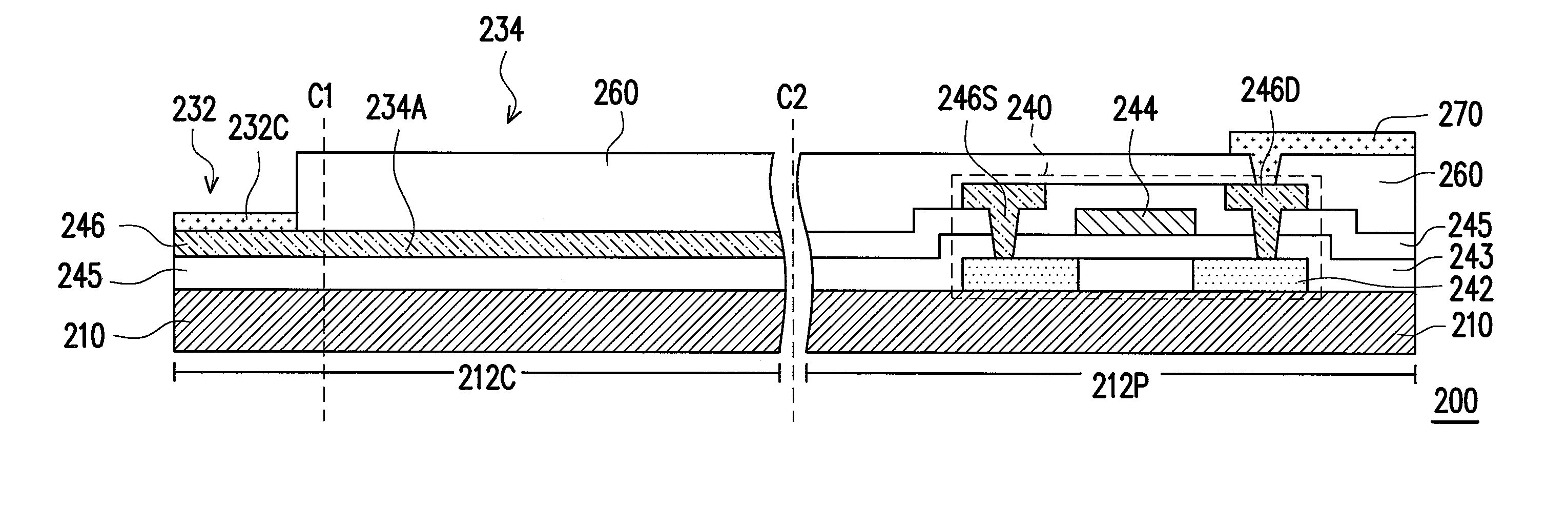
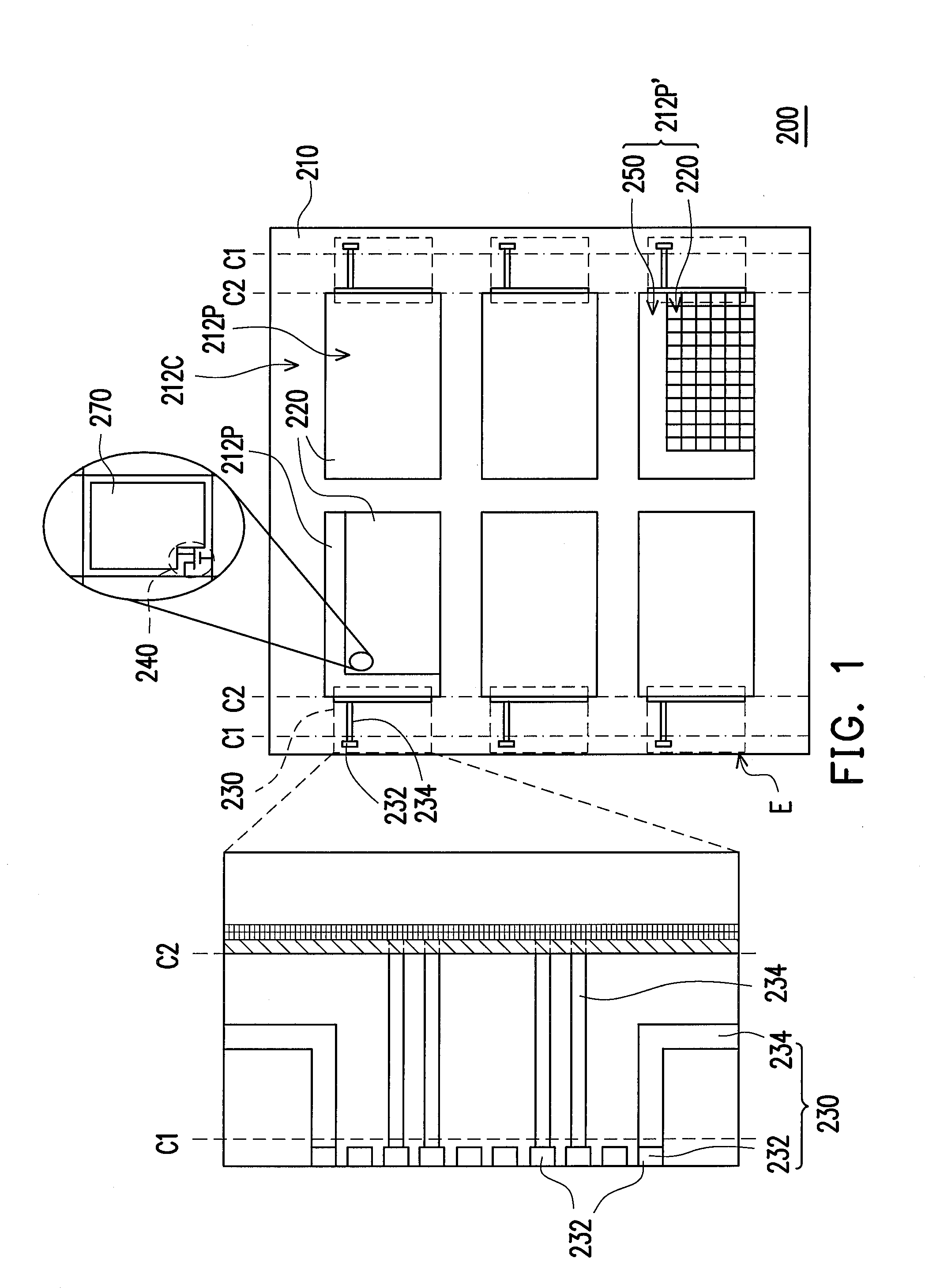
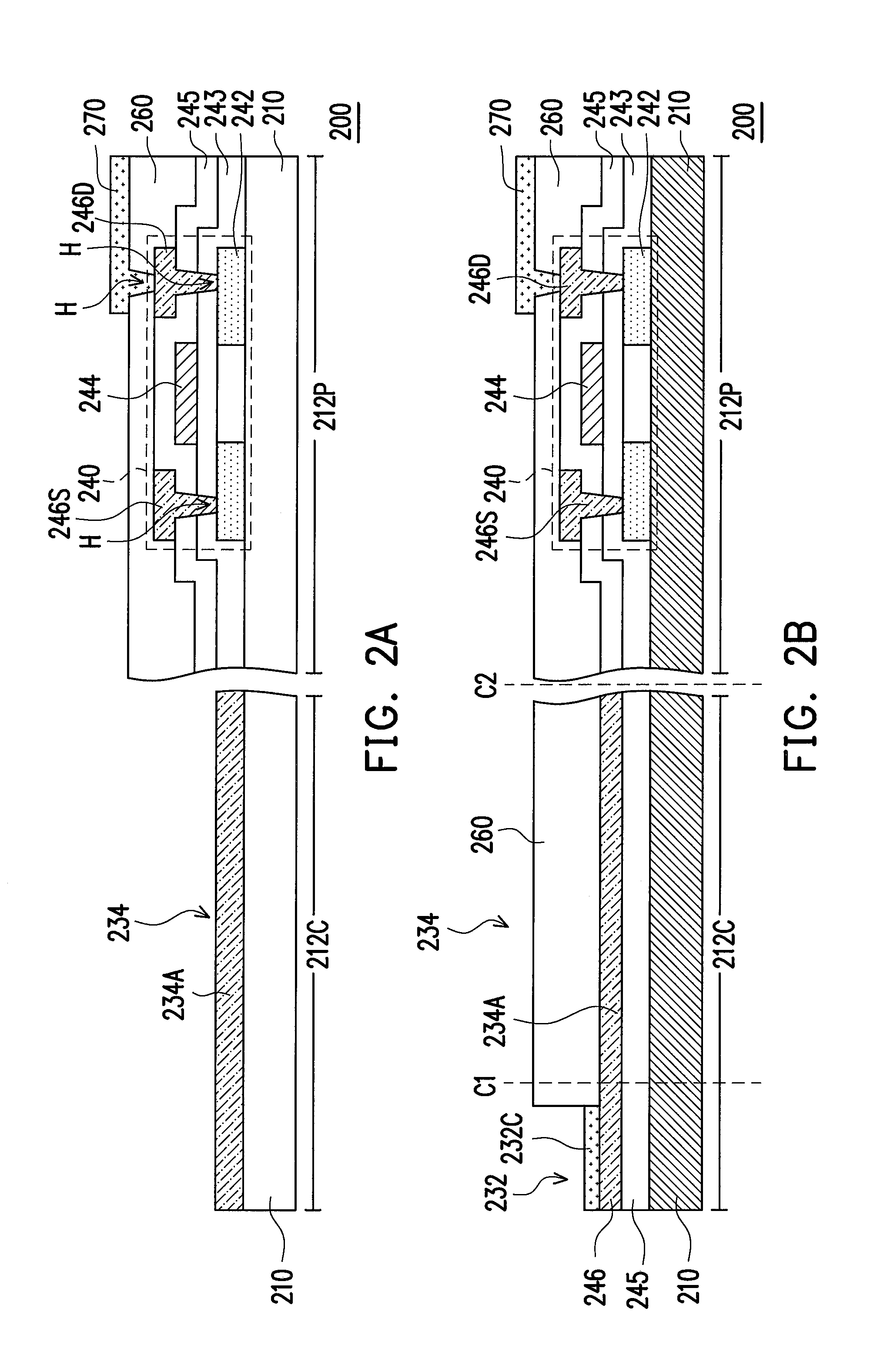
[0031]The invention is directed to a polymer-stabilized alignment (PSA) curing circuit disposed on an active device array mother substrate. In existing fabrication processes, for the consideration of circuit layout on a substrate and the buffering of impacts from various processes to curing lines, the active device array mother substrate in the invention adopts a suitable layer as curing lines to avoid an effect of a subsequent process, such as a doping process, on conventional curing lines, thereby preventing the peeling of the curing lines. In a method of fabricating a display panel of the invention, a forming process of curing lines is performed after a doping process of active devices, so that the peeling of conventional curing lines can be solved effectively.

[0032]To better elaborate the curing lines and the active device array mother substrate adopting the curing lines in the invention, several embodiments are accompanied with figures to further illustrate the invention in det...


PUM


Abstract

An active device array mother substrate including a substrate, pixel arrays, and a polymer-stabilized alignment curing circuit is provided. The substrate has panel regions, a circuit region, a first cutting line, and a second cutting line. The first cutting line is disposed on the circuit region between an edge of the substrate and the second cutting line. The active devices of the pixel arrays have a semiconductor layer. The polymer-stabilized alignment curing circuit disposed on the circuit region includes curing pads disposed between the edge of the substrate and the first cutting line and curing lines having an upper conductive layer connected to the corresponding curing pads and the corresponding pixel array. The upper conductive layer is in the same layer as the source / drain conductor. Therefore, the curing lines are capable of preventing problems such as peeling, so as to keep the polymer-stabilized alignment curing circuit operating normally.

Description

CROSS-REFERENCE TO RELATED APPLICATION[0001]This application claims the priority benefit of Taiwan application serial no. 98129453, filed Sep. 1, 2009. The entirety of the above-mentioned patent application is hereby incorporated by reference herein and made a part of specification.BACKGROUND OF THE INVENTION[0002]1. Field of the Invention[0003]The invention relates to a substrate and a method of fabricating a display apparatus, and more particularly relates to an active device array mother substrate and a method of fabricating a display panel.[0004]2. Description of Related Art[0005]With the increase in computing power and the rapid development of internet and multimedia technologies, sizes of video or image apparatuses are miniaturized gradually. In the development of displays, along with the progress in optoelectronic technology and semiconductor fabrication technology, liquid crystal displays (LCDs) with superior features such as high definition, great space utilization, low pow...

Claims


Application Information

Patent Timeline
Patent Type & Authority Applications(United States)
IPC IPC(8): H01L33/00H01L21/30
CPCG02F1/133351G02F1/133703H01L27/1214G02F1/13458G02F1/133788
Inventor CHEN, YU-MOUHSU, WEN-BINCHAO, CHIH-YAOHSU, TSUNG-YI
Owner AU OPTRONICS CORP
Why Eureka
Try Eureka