
Solar cell and fabricating method thereof

Inactive Publication Date: 2011-03-03
LG ELECTRONICS INC
View PDF10 Cites 11 Cited by
  • Summary
  • Abstract
  • Description
  • Claims
  • Application Information

AI Technical Summary

Benefits of technology

[0011]An object of the present invention is to provide a fabricating method of a solar cell, and particularly a structure and process of the solar cell in which formation of electrodes is improved, thereby being environmentally friendly, stabilizing the process, reducing process costs, and achieving mass production of the high-efficiency solar cell.
[0012]Another object of the present invention is to provide a solar cell including improved electrodes in terms of a material, which maintains reliability in quality of the solar cell without lowering the efficiency of the solar cell, and does not cause environmental pollution.
[0021]The second conductivity-type semiconductor layer may be the n+-type emitter doped with a high concentration of the n-type impurity. A doping concentration of the n+-type emitter is not limited to a specific level, but may be 1×10¹⁹˜1×10²¹ atom / cm3. By doping the n+-type emitter with a high concentration of the n-type impurity, the sheet resistance of the n+-type emitter may be lowered, thereby improving contact efficiency with metal electrodes. The sheet resistance of the n+-type emitter is not limited to a specific level, but may be about 30˜100 Ω / square.
[0023]Particularly, the formation of the at least one front electrode of the solar cell in accordance with the present invention is not achieved by a general fire-through process, and thus may prevent or reduce generation of short circuit of front electrodes through an ultra-thin second conductivity-type semiconductor layer during formation of the front electrodes of a conventional solar cell. Therefore, although the second conductivity-type semiconductor layer of the solar cell of the present invention is formed in an ultra-thin type, the at least one front electrode may be easily formed without any short circuit. In order to more firmly prevent the short circuit, the thickness of the second conductivity-type semiconductor layer in a region of which that contacts the at least one front electrode may be smaller than the thickness of the second conductivity-type semiconductor layer in regions of which that do not contact the at least one front electrode.

Problems solved by technology

Fossil fuels are expected to run out several years from now, and simultaneously, environmental problems, such as global warming, due to discharge of carbon dioxide according to use of a large amount of fossil fuels are on the rise.

Method used


Image

  • Solar cell and fabricating method thereof
  • Solar cell and fabricating method thereof
  • Solar cell and fabricating method thereof

Examples


Embodiment Construction

[0053]The advantages and features of the present invention, and the way of attaining them, will become apparent with reference to embodiments described below in conjunction with the accompanying drawings.

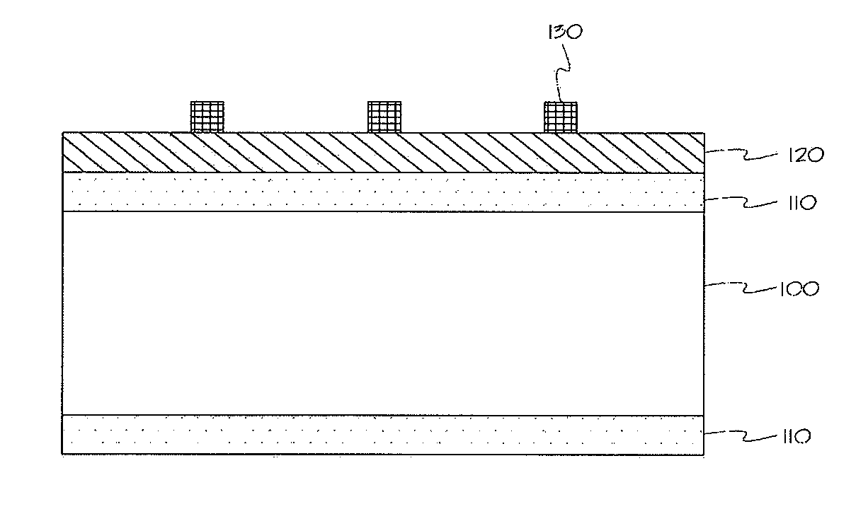
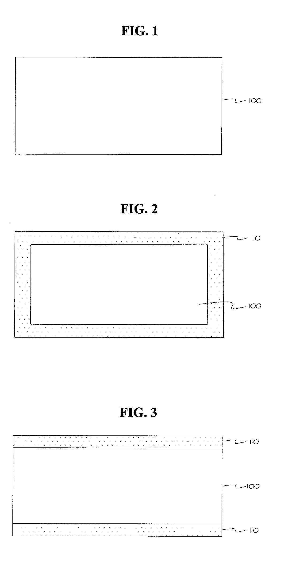
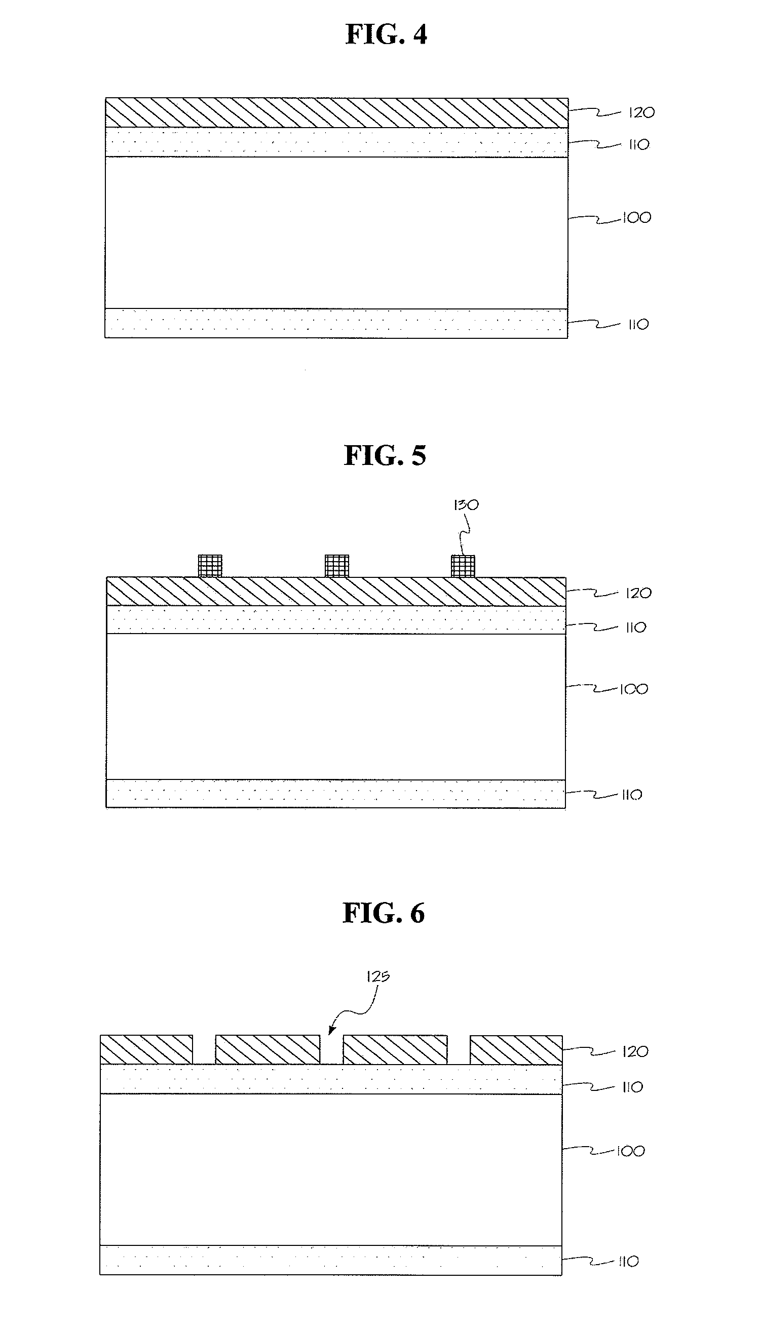
[0054]FIGS. 1 to 9 are sectional views sequentially illustrating a fabricating method of a solar cell in accordance with embodiments of the present invention.

[0055]FIGS. 1 to 8 are sectional views schematically illustrating a fabricating process of a completed solar cell shown in FIG. 9. Embodiments of the solar cell are not limited thereto, but may be fabricated through various processes which do not deviate from the technical scope of embodiments of the present invention.

[0056]First, as shown in FIG. 1, a substrate 100 (also referred to as a p-type semiconductor substrate 100) is prepared by doping a semiconductor substrate with a p-type semiconductor impurity. Examples of the semiconductor for the p-type semiconductor substrate 100 may be silicon.

[0057]In FIG. 1, texturing of the...


PUM


Abstract

Discussed herein are a solar cell and a fabricating method thereof. The solar cell includes a first conductivity-type semiconductor substrate, a second conductivity-type semiconductor layer formed on a front surface of the first conductivity-type semiconductor substrate, and having a conductivity opposite to that of the first conductivity-type semiconductor substrate, an anti-reflection film including at least one opening exposing a part of a surface of the second conductivity-type semiconductor layer, and formed on the second conductivity-type semiconductor layer, at least one front electrode contacting a part of the surface of the second conductivity-type semiconductor layer exposed through the at least one opening, and at least one rear electrode formed on a rear surface of the first conductivity-type semiconductor substrate, wherein the at least one front electrode includes a metal containing silver and lead-free glass frit.

Description

[0001]This application claims priority to and the benefit of Korean Patent Application No. 10-2009-0079934, filed on Aug. 27, 2009 in the Korean Intellectual Property Office, the disclosure of which is incorporated herein by reference.BACKGROUND OF THE INVENTION[0002]1. Field of the Invention[0003]Embodiments of the present invention relate to a solar cell and a fabricating method thereof, and more particularly to a fabricating method of a solar cell for producing the solar cell having a reliable quality and a high efficiency with a high yield, and reduce process costs while preventing or reducing environmental pollution.[0004]2. Discussion of the Related Art[0005]Recently, as exhaustion of existing energy resources, such as oil and coal, is expected, there is increasing interest in alternative energy sources. Among them, solar cells are a source of abundant energy and do not cause environmental pollution, and thus, are attracting wide attention. Types of solar cells include a solar...

Claims


Application Information

Patent Timeline
IPC IPC(8): H01L31/0224H01L31/0216H01L31/18H01L31/0236H01L31/068
CPCH01L31/022425H01L31/068Y02E10/52H01L31/022441H01L31/02167H01L31/1804Y02E10/547Y02E10/542Y02P70/50H01L31/04
Inventor LEE, SEONGEUNJEONG, JIWEON
Owner LG ELECTRONICS INC
Learn More