
Photoelectric conversion device and manufacturing method thereof

Inactive Publication Date: 2011-02-24
SEMICON ENERGY LAB CO LTD
View PDF33 Cites 27 Cited by
  • Summary
  • Abstract
  • Description
  • Claims
  • Application Information

AI Technical Summary

Benefits of technology

[0017]In view of the foregoing problems, an object of one embodiment of the present invention is to provide a photoelectric conversion device of resource saving type making good use of a semiconductor material. Another object of one embodiment of the present invention is to provide a photoelectric conversion device with high mechanical strength and improved photoelectric conversion efficiency. Another object of one embodiment of the present invention is to provide a manufacturing method of the above photoelectric conversion device.
[0024]Light which enters the single crystal semiconductor layer through the light-transmitting base substrate is repeatedly scattered by a light-trapping effect which is caused by the first plurality of depressions and / or the second plurality of depressions, whereby photo-carriers can be efficiently generated.
[0028]According to one embodiment of the present invention, a high-efficiency and resource-saving photoelectric conversion device with high mechanical strength in which a transparent insulating substrate is used as a support substrate can be provided. In addition, a manufacturing method of the photoelectric conversion device can be provided.

Problems solved by technology

However, although single crystals are structured by orderly arranged atoms. single crystals may include disorder such as a lattice defect in which the alignment is partially disordered or intended or unintended lattice distortion.

Method used


Image

  • Photoelectric conversion device and manufacturing method thereof
  • Photoelectric conversion device and manufacturing method thereof
  • Photoelectric conversion device and manufacturing method thereof

Examples


embodiment 1

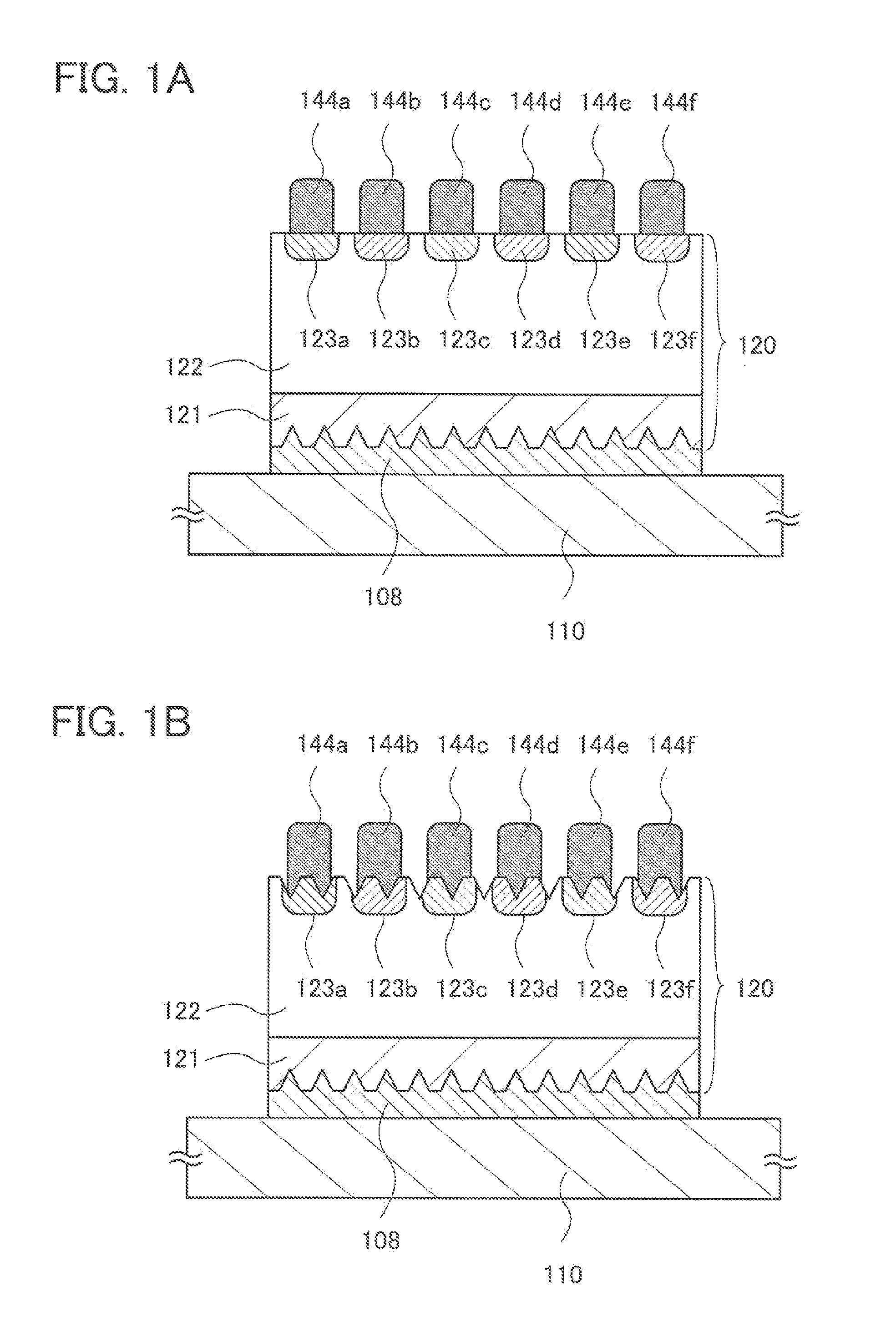
[0050]One embodiment of the present invention relates to a photoelectric conversion device having a single crystal semiconductor layer. In the photoelectric conversion device, a light-transmitting insulating substrate is used as a support substrate, semiconductor junction and electrodes are formed on the semiconductor layer surface side, and a light-receiving surface is the supporting substrate side.

[0051]A cross-sectional view of a photoelectric conversion device in which a photoelectric conversion layer is provided over a base substrate is illustrated in FIG. 1A. There are no particular limitations on the planar shape of the photoelectric conversion layer, and a rectangular shape such as a square, a polygonal shape, or a circular shape can be employed.

[0052]There are no particular limitations on a base substrate 110 as long as the substrate can withstand a manufacturing process of the photoelectric conversion device according to one embodiment of the present invention and transmit...

embodiment 2

[0173]One embodiment of the present invention relates to a photoelectric conversion device having a single crystal semiconductor layer. In the photoelectric conversion device, a light-transmitting insulating substrate is used as a support substrate, semiconductor junction and electrodes are formed on the semiconductor layer surface side, and a light-receiving surface is the supporting substrate side.

[0174]In this embodiment, a method for manufacturing a photoelectric conversion module will be described in details with reference to drawings.

[0175]FIG. 8 illustrates an example in which a plurality of planar photoelectric conversion layers are arranged over one substrate having an insulating surface at predetermined intervals. In the example, electrodes are formed for a plurality of photoelectric conversion layers and they are connected in series to form a unit and the units are connected in parallel. A positive terminal and a negative terminal which extract power from the photoelectri...

embodiment 3

[0203]In this embodiment, an example of a photoelectric conversion device and a manufacturing method thereof which is different from that described in Embodiment 2 will be described. Note that a description of the same components as those of the above embodiment is omitted or partly simplified.

[0204]By the steps according to Embodiment 1, stacked layers including the insulating layer 108, the first single crystal semiconductor layer 121, and the second single crystal semiconductor layer 122 are formed over the base substrate 110 (see FIG. 5B).

[0205]Over the stacked layers, first impurity semiconductor layers 230a, 230c, and 230e and second impurity semiconductor layers 230b, 230d, and 230f are alternately formed in stripes without overlapping with each other. Over the impurity semiconductor layers, first electrodes 240a, 240e, and 240e and second electrodes 240b, 240d, and 240f are formed, whereby the photoelectric conversion device can be completed (see FIGS. 11A, 11B, and 11C and ...


PUM


Abstract

A novel photoelectric conversion device and a manufacturing method thereof are provided. The photoelectric conversion device includes an insulating layer over a light-transmitting base substrate; a single crystal semiconductor layer provided with a plurality of depressions which are filled with the insulating layer; a plurality of first impurity semiconductor layers formed in stripes having one conductivity type and a plurality of second impurity semiconductor layers formed in stripes having a conductivity type which is opposite to the one conductivity type, which are arranged alternately and do not overlap with each other, in a surface layer or over a surface of the single crystal semiconductor layer; first electrodes which are in contact with the first impurity semiconductor layers; and second electrodes which are in contact with the second impurity semiconductor layers.

Description

BACKGROUND OF THE INVENTION[0001]1. Field of the Invention[0002]The present invention relates to a photoelectric conversion device and a manufacturing method thereof.[0003]2. Description of the Related Art[0004]Global warming has become a serious problem, and the active use of energy sources which will replace fossil fuels has started to spread. In recent years, research and development on photoelectric conversion devices, which are also called solar cells, have become very active, and the market is rapidly expanding.[0005]The photoelectric conversion devices are very attractive power generation means which use inexhaustible sunlight as the energy source and which do not emit carbon dioxide at the time of power generation. However, there are problems under present conditions in that photoelectric conversion efficiency per unit area is not sufficient, that the amount of power generation is affected by the daylight hours, and the like. Accordingly, a long time of around 20 years is ne...

Claims


Application Information

Patent Timeline
IPC IPC(8): H01L31/036H01L31/18
CPCH01L31/022441H01L31/02363H01L31/02366Y02E10/547H01L31/1804H01L31/1892H01L31/0682Y02P70/50
Inventor SHIMOMURA, AKIHISAKATO, SHOHIURA, YOSHIKAZU
Owner SEMICON ENERGY LAB CO LTD
Learn More