Method and apparatus for fabricating optoelectromechanical devices by structural transfer using re-usable substrate

a technology of optoelectromechanical devices and re-usable substrates, applied in the direction of electrical apparatus, semiconductor devices, nanotechnology, etc., can solve the problems of unpredictable performance degradation, substantial cost, and limited technology of each fabrication technique of combining two or more different materials on a single substrate, and achieve the effect of low cos

Inactive Publication Date: 2011-02-17
RGT UNIV OF CALIFORNIA
View PDF4 Cites 82 Cited by
  • Summary
  • Abstract
  • Description
  • Claims
  • Application Information

AI Technical Summary

Benefits of technology

This patent describes a method for transferring structures from one substrate to another, while preserving the integrity and fidelity of the transferred structures. This is achieved by using a process that involves embossing, imprinting, or embedding the structures into a separate carrier substrate while applying physical motions or forces that exceed the critical material stress limit of the structures. This method offers a universal platform for material integration and can be used in several areas of micro / nanoscale electronics and photonics. The transferred structures can be used to create multifunctional optoelectromechanical devices with low dark current, reduced parasitic capacitance, and higher efficiency of light absorption. The process is cost-effective and can be used for large-scale production of devices.

Problems solved by technology

However, each of these fabrication techniques of combining two or more different materials on a single substrate has been limited by technological challenges.
These challenges include, but are not limited to, CMOS incompatibility due to extreme physical growth conditions such as high temperature; the loss of complete starting substrates which leads to substantial cost; and the interface defects, vacancies, and traps in heteroepitaxy of mismatched materials which results in unpredictable performance degradation.
Unfortunately, all of these transfer techniques either do not preserve the original orientation of the array structural order on the carrier substrate or have been limited to two-dimensional (2-D) crystal film transfer.
In some embodiments, the process fractures the structures of the multiple devices off the first substrate by causing a relative motion between the first substrate and the second substrate, wherein the relative motion causes a stress-strain induced mechanical failure of the structures in the vicinity where the structures join the first substrate.

Method used


Image

  • Method and apparatus for fabricating optoelectromechanical devices by structural transfer using re-usable substrate
  • Method and apparatus for fabricating optoelectromechanical devices by structural transfer using re-usable substrate
  • Method and apparatus for fabricating optoelectromechanical devices by structural transfer using re-usable substrate

Examples


Embodiment Construction

[0137]The following description is presented to enable any person skilled in the art to make and use the embodiments, and is provided in the context of a particular application and its requirements. Various modifications to the disclosed embodiments will be readily apparent to those skilled in the art, and the general principles defined herein may be applied to other embodiments and applications without departing from the spirit and scope of the present disclosure. Thus, the present invention is not limited to the embodiments shown, but is to be accorded the widest scope consistent with the principles and features disclosed herein.

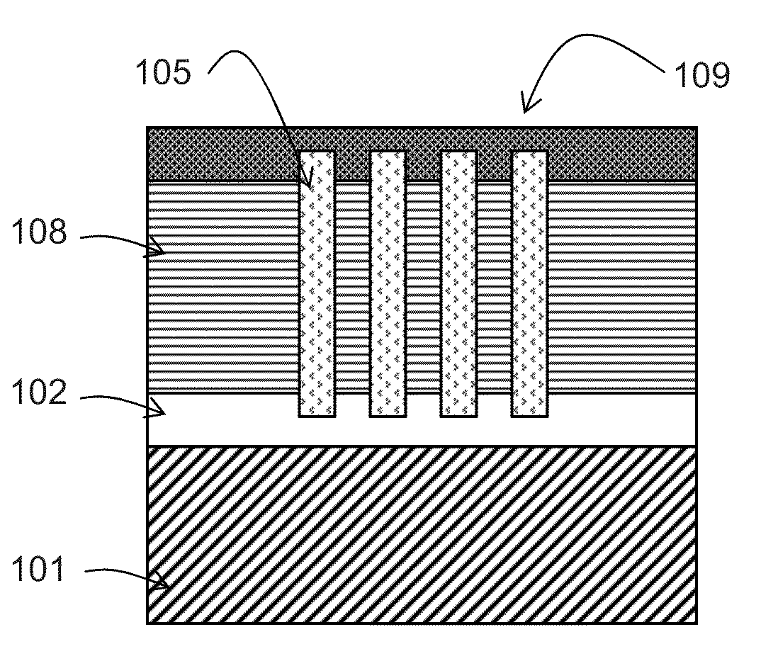
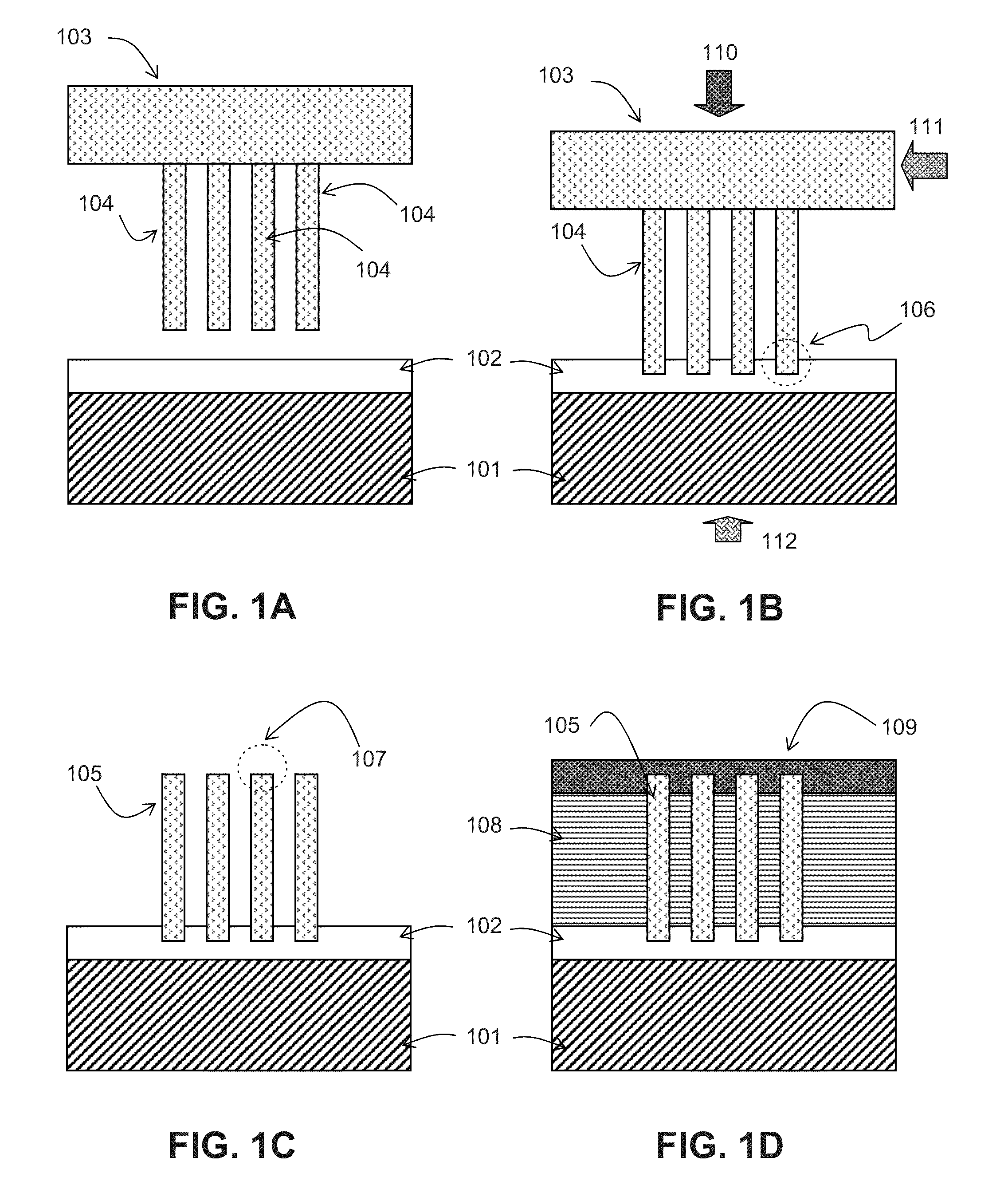
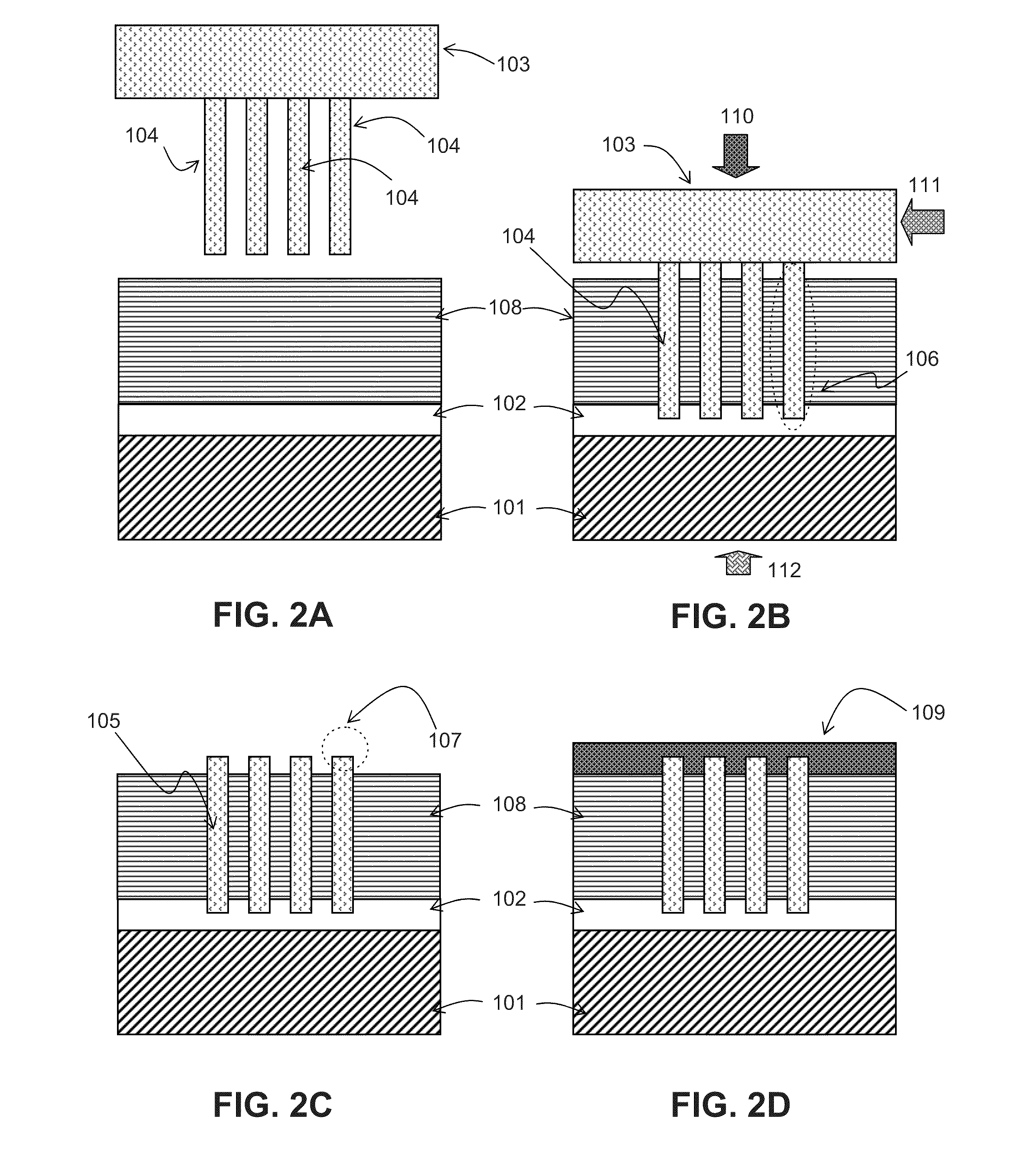
[0138]In the following discussion, note that like reference numerals refer to corresponding parts throughout the drawings. Furthermore, the same drawing numeral labeling appearing in more than one drawing refers to the same element. In addition, hereinafter, the following definitions apply:

[0139]“Mother substrate” refers to an original substrate or templat...


PUM


Abstract

One embodiment of the present invention provides a process for fabricating multiple devices on a single substrate based on a structure transfer process. During operation, the process starts by forming structures of multiple devices on a first substrate. The process then bonds the structures of the multiple devices onto a second substrate. Next, the process transfers the multiple devices from the first substrate onto the second substrate by fracturing the structures of the multiple devices off the first substrate, wherein the transferred devices preserve physical orientation and material properties of the said fabricated structures.

Description

BACKGROUND[0001]1. Field of the Invention[0002]The present invention generally relates to the field of material or structure transfer and more specifically to manufacturing optoelectromechanical devices which involves the process of transferring structures from a mother substrate to a carrier substrate.[0003]2. Related Art[0004]Semiconductor-based electronics and photonics devices have made significant impact in communication and computing technologies. Meanwhile, rapid advances in these technologies are driving demands for monolithic integration of multifunctional materials and devices on a single substrate. These monolithically integrated materials and devices typically are associated with diverse bandgap, electrical and optical properties, and thus could offer solutions to a wide range of technological challenges, for example, in multifunctional material integration for CMOS-compatible electronics and photonics.[0005]Significant progress in material synthesis and device integrati...

Claims


Application Information

Patent Timeline
Patent Type & Authority Applications(United States)
IPC IPC(8): H01L31/0352H01L21/50H01L31/18
CPCB82Y10/00H01L21/02603H01L21/02606H01L31/0352H01L29/0673H01L29/0676H01L29/125H01L29/0665
Inventor JAYARAMAN, LOGEESWARAN VEERAYAHKATZENMEYER, AARON M.ISLAM, M. SAIF
Owner RGT UNIV OF CALIFORNIA
Why Eureka
Try Eureka