Thin film transistor substrate and thin film transistor used for the same
a thin film transistor and substrate technology, applied in the direction of transistors, electrical devices, semiconductor devices, etc., can solve the problems of more manufacturing process, disadvantageous structure in view of production cost, and difficulty in forming such a
- Summary
- Abstract
- Description
- Claims
- Application Information
AI Technical Summary
Benefits of technology
Problems solved by technology
Method used
Image

Examples
exemplary embodiment 1
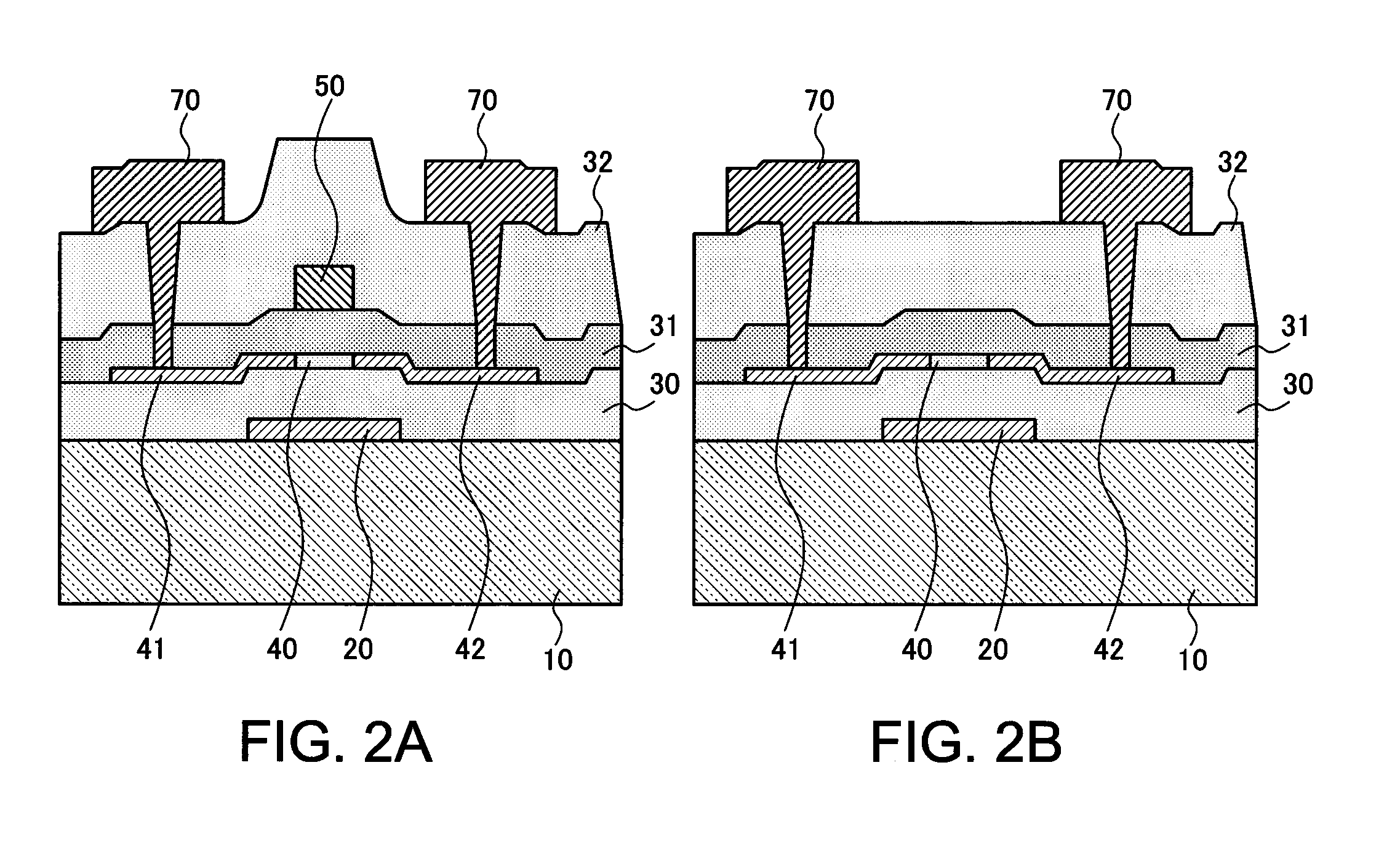
Referring to FIG. 2A and FIG. 2B, the first exemplary embodiment of the present invention will be described wherein a first TFT having a relatively low breakdown voltage capability and a second TFT having a breakdown voltage capability higher than that of the first TFT are formed on the same substrate for providing a TFT circuitry substrate.
As shown in FIG. 2A and FIG. 2B, each bottom gate electrode 20 is formed on a first TFT area and a second TFT area of a common insulating substrate 10, respectively, and a bottom gate insulating film 30 is formed commonly on the bottom gate electrode 20. The bottom gate insulating film 30 is made relatively thick so as to correspond to a driving voltage applied to the second TFT. Each semiconductor layer 40 is formed on the bottom gate insulating film 30 such that a source region 41 and a drain region 42 are provided for both TFTs, respectively. Then a top gate insulating film 31 is formed to cover the semiconductor layer 40. The top gate insulat...
exemplary embodiment 2
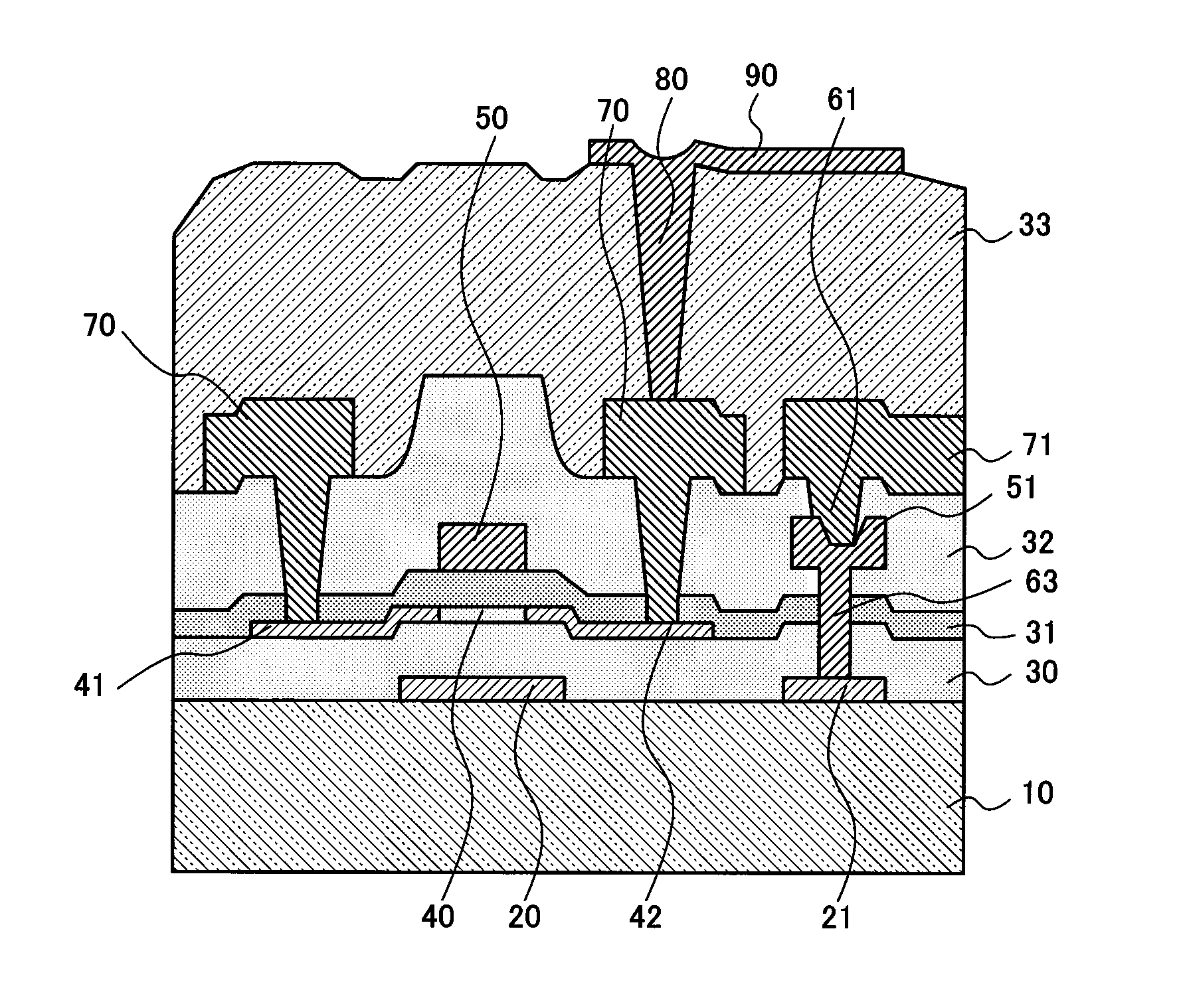
In the first exemplary embodiment mentioned above, although a case when the source / drain electrode wirings 70 are located above the top gate electrode is indicated, the second exemplary embodiment shown in FIG. 7 has a configuration such that the source / drain electrode wirings 70 are located below the top gate electrode. That is, according to the second exemplary embodiment, the source / drain electrode wirings 70 are formed prior to forming the top gate insulating film 31. By this method, a process needed to form the contact holes 60 shown in the configuration of FIG. 2 can be omitted. A contact hole 160 is formed instead of a contact hole 61 shown in FIG. 2 so that the electrode 21 formed on the same layer of the bottom gate electrode 20 is connected to the contact hole 160. That is, an opening for the contact hole 160 is formed into both of the bottom gate insulating film 30 and the top gate insulating film 31 prior to forming the top gate electrode 50. And thus the top gate electr...
exemplary embodiment 3
In the third exemplary embodiment of the present invention, it is described about a configuration which applied the present invention to TFT having offset configurations. As shown in FIG. 9 through FIG. 13, it is possible to provide both TFTs of the low voltage TFT and the high voltage TFT on the same substrate easily and simultaneously. In FIG. 9 and FIG. 10, one example in accordance with the first exemplary embodiment and another example in accordance with the second exemplary embodiment are indicated, respectively, and thereby showing a TFT substrate with the combination structure of the low voltage TFT (or high current driving TFT) and the high voltage TFT (or high breakdown voltage capability TFT) on the same substrate, and either one of such configurations can be adopted appropriately for the TFT substrate circuitry. In the same manner, FIG. 11 and FIG. 12 show two examples, respectively. One example shown in FIG. 11A and FIG. 11B is associated with the first exemplary embodi...
PUM
 Abstract
Description
Claims
Application Information
 - R&D
- Intellectual Property
- Life Sciences
- Materials
- Tech Scout
- Unparalleled Data Quality
- Higher Quality Content
- 60% Fewer Hallucinations
Browse by: Latest US Patents, China's latest patents, Technical Efficacy Thesaurus, Application Domain, Technology Topic, Popular Technical Reports.
© 2025 PatSnap. All rights reserved.Legal|Privacy policy|Modern Slavery Act Transparency Statement|Sitemap|About US| Contact US: help@patsnap.com