Glass substrate for display device, liquid crystal display panel, and liquid crystal display device
- Summary
- Abstract
- Description
- Claims
- Application Information
AI Technical Summary
Benefits of technology
Problems solved by technology
Method used
Image
Examples
Embodiment Construction
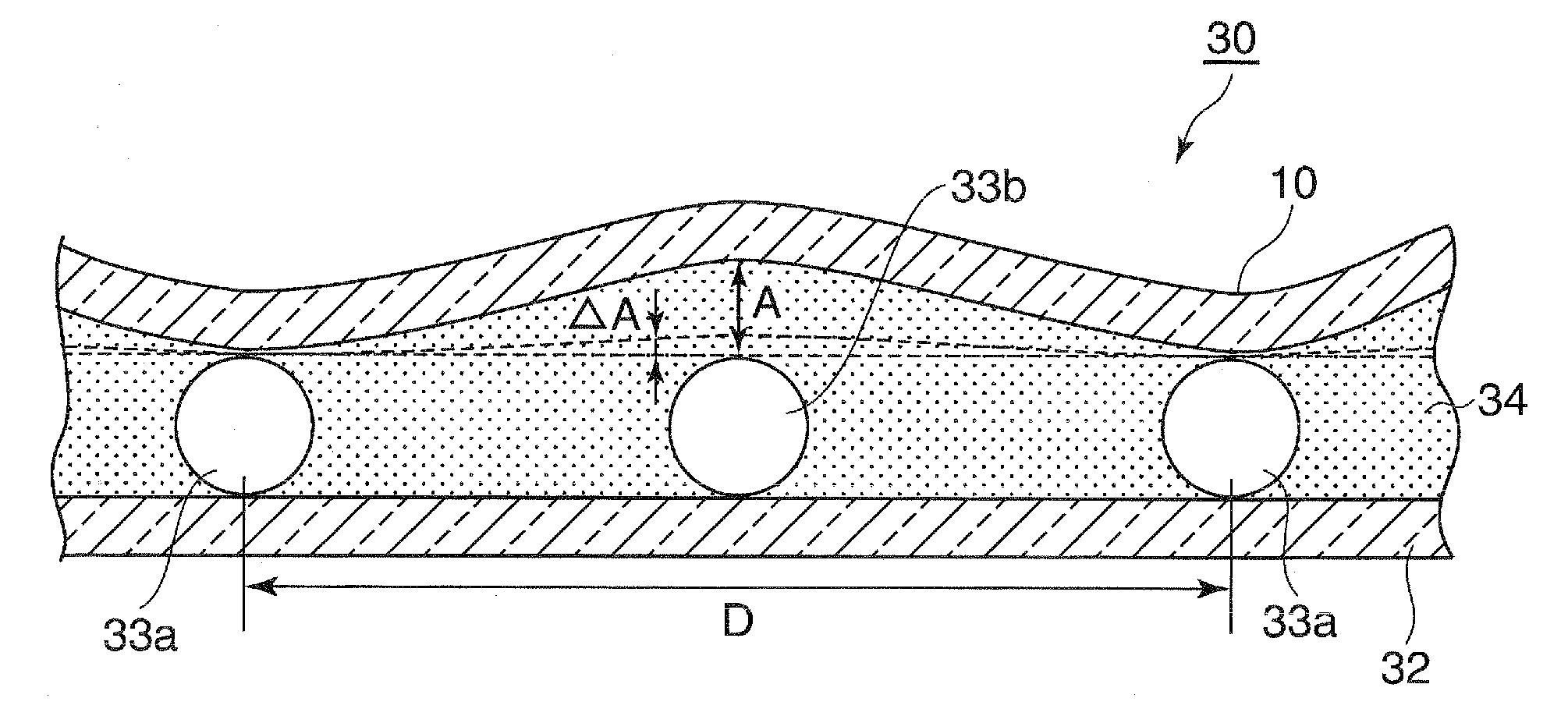
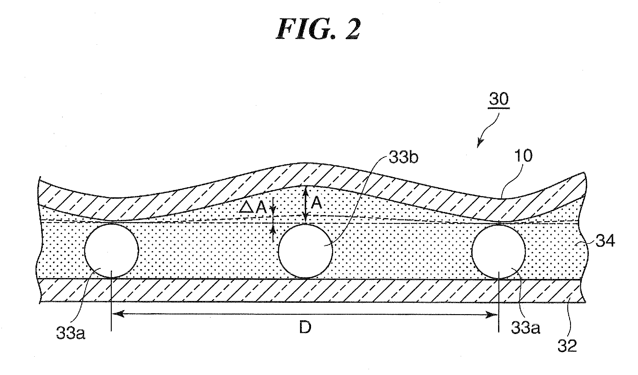
[0025]The present inventors have made intensive studies in order to achieve the above-mentioned object, and as a result, they have found that in at mm-thick glass substrate for a display device fabricated by applying tensile stress to plate-like glass having an equilibrium thickness in two directions in plane with a surface of the glass and perpendicular to each other, if, when a period D of a filtered waviness curve over a spatial frequency range of 2 to 500 lines / mm based on spectral analysis is greater than 20 mm under the measurement condition of a cut-off value of 0.8 to 8 mm, an amplitude A of the filtered waviness curve is 2×(1.1 / t)3 μm or less, and if the amplitude A, when the period D is 20 mm or less and t is 1.1 mm, is 18 nm or greater, it is possible to eliminate the display unevenness of a liquid crystal panel after the glass substrate is assembled thereinto (hereinafter referred to as “the cell assembly”), and eliminate the need for a post-process or simplify the post-...
PUM
| Property | Measurement | Unit |
|---|---|---|
| Length | aaaaa | aaaaa |
| Length | aaaaa | aaaaa |
| Length | aaaaa | aaaaa |
Abstract
Description
Claims
Application Information
 - R&D
- Intellectual Property
- Life Sciences
- Materials
- Tech Scout
- Unparalleled Data Quality
- Higher Quality Content
- 60% Fewer Hallucinations
Browse by: Latest US Patents, China's latest patents, Technical Efficacy Thesaurus, Application Domain, Technology Topic, Popular Technical Reports.
© 2025 PatSnap. All rights reserved.Legal|Privacy policy|Modern Slavery Act Transparency Statement|Sitemap|About US| Contact US: help@patsnap.com


