Device

Inactive Publication Date: 2011-01-06
ELPIDA MEMORY INC
View PDF2 Cites 2 Cited by
  • Summary
  • Abstract
  • Description
  • Claims
  • Application Information

AI Technical Summary

Benefits of technology

[0011]Provision of a protection insulation film on the upper side of a region interposed between the gate insulation film and the isolation insulation region increases the distance between the top face of the active region located in the lower side of that region and the gate insulation film and gate electrode, whereby the local concentration of the electric field in the active region is prevented. If the electric field is blocked from the top face, the channel region width will be decreased by that much and the drive current of the transistor will be reduced. However, the occupancy of the top face to the total width of the channel region is rather low and the occupancy will be decreased along with further downsizing of semiconductor devices in the future. Therefore, even if a semiconductor device is configured such that the electric field is not generated from the top face of the channel region like the one according to an embodiment of the invention, the drive current of the transistor will not change significantly in comparison with the case in which the electric field is generated from the top face.

Problems solved by technology

However, when an attempt is made to reduce the size of a planar field-effect transistor, a short-channel effect will occur due to reduced gate width.
Furthermore, the channel region width also will be reduced, causing a problem of reduced drive current.
Therefore, it is difficult to reduce the size of planar field-effect transistors.
This means that the electric field generated in this configuration is increased in a manner concentrated particularly to the vicinity of the tip end of the projecting part, possibly resulting in deterioration of dielectric voltage of the gate oxide film and eventually dielectric breakdown.

Method used


Image

  • Device
  • Device
  • Device

Examples


Embodiment Construction

[0023]The invention will be now described herein with reference to illustrative embodiments. Those skilled in the art will recognize that many alternative embodiments can be accomplished using the teachings of the present invention and that the invention is not limited to the embodiments illustrated for explanatory purposes.

[0024]In the following, a DRAM (Dynamic Random Access Memory) is used as an example of devices, and description will be made of a manufacturing process of a transistor such as a MOSFET (Metal Oxide Semiconductor Field Effect Transistor) used in the DRAM.

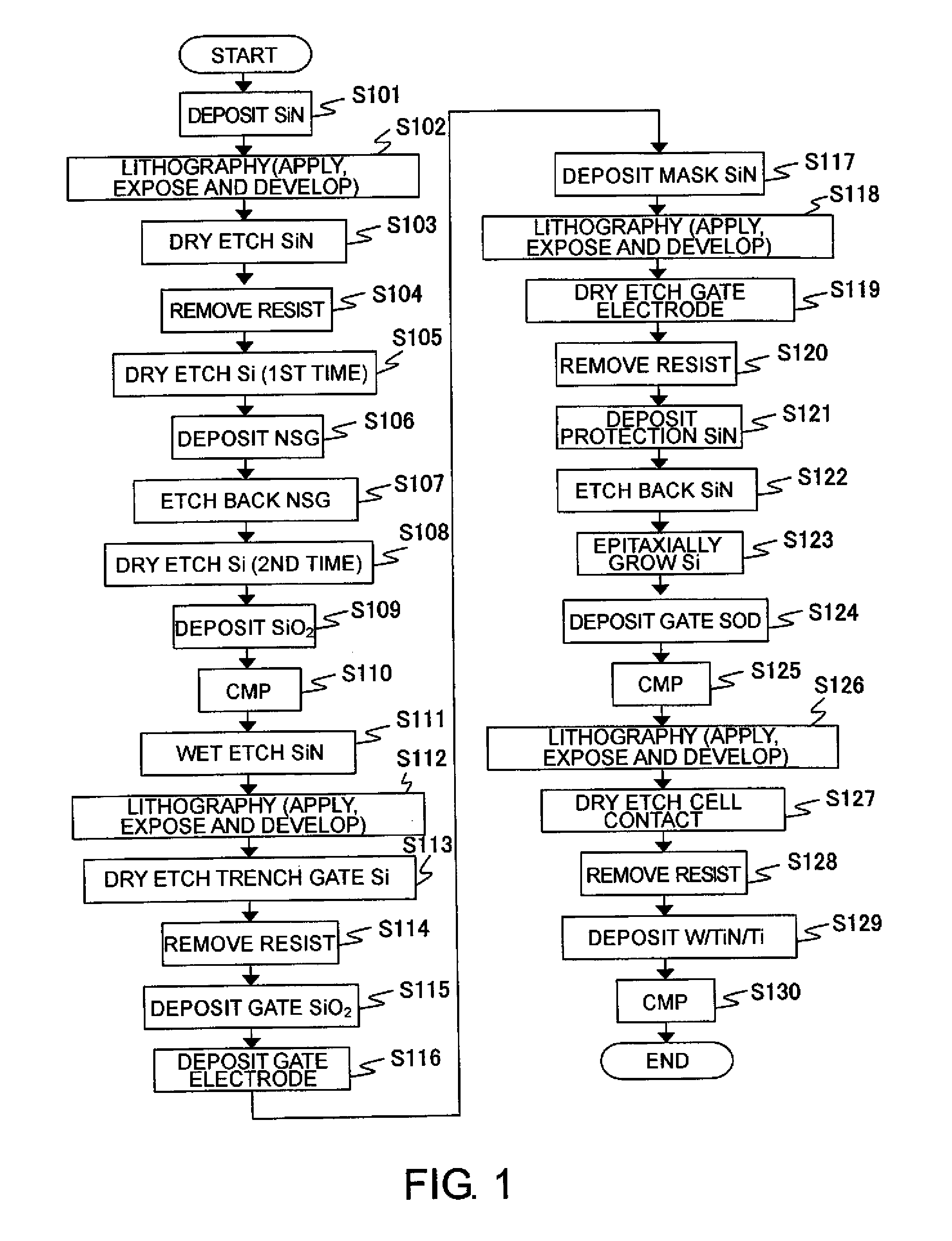
[0025]FIG. 1 is a flowchart for explaining a first example of a manufacturing process of a MOSFET. It should be noted that this flowchart shows only steps of forming principal components (e.g. STI (Shallow Trench Isolation), gate electrode, and cell contact), while omitting the steps of impurity diffusion and so on which can be performed by using the known methods.

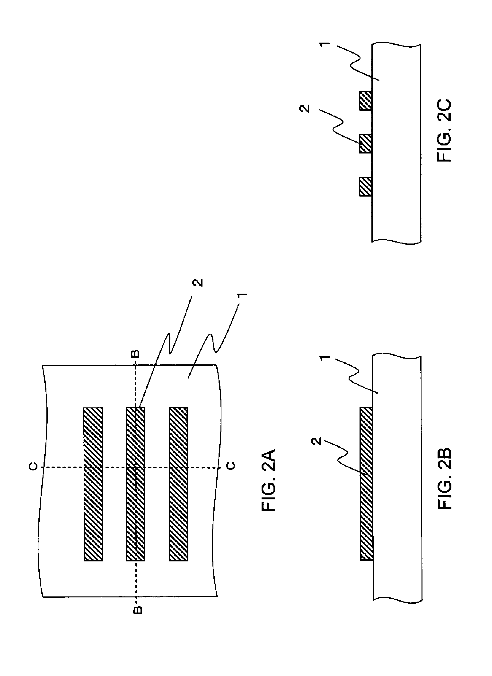
[0026]Referring to FIGS. 2A to 2C through FIGS. 10...


PUM


Abstract

A semiconductor device includes a first diffusion region and a second diffusion region in an active region surrounded by an isolation insulation region, a recessed trench region formed between the first diffusion region and the second diffusion region, a gate insulation film formed on the trench region, a gate electrode formed on the gate insulation film to fill the trench region therewith, and a protection insulation film formed in an upper part of the region interposed between the gate insulation film and the isolation insulation region.

Description

[0001]This application is based upon and claims the benefit of priority from Japanese patent application No. 2009-158345, filed on Jul. 3, 2009, the disclosure of which is incorporated herein in its entirety by reference.BACKGROUND OF THE INVENTION[0002]1. Field of the Invention[0003]This invention relates to a device and a manufacturing method thereof, and in particular relates to a semiconductor device having a field-effect transistor and a manufacturing method thereof.[0004]2. Description of the Related Art[0005]High degree integration of semiconductor devices requires size reduction of transistors. However, when an attempt is made to reduce the size of a planar field-effect transistor, a short-channel effect will occur due to reduced gate width. Furthermore, the channel region width also will be reduced, causing a problem of reduced drive current. Therefore, it is difficult to reduce the size of planar field-effect transistors.[0006]Known methods for enabling reduction of the tr...

Claims


Application Information

Patent Timeline
IPC IPC(8): H01L29/78
CPCH01L21/3083H01L21/76229H01L29/1037H01L29/78H01L29/66621H01L29/66628H01L29/4236
Inventor MIKASA, NORIAKI
Owner ELPIDA MEMORY INC
Why Eureka
Try Eureka