Multi-Bank Non-Volatile Memory System with Satellite File System

a multi-bank, non-volatile technology, applied in memory address/allocation/relocation, program control, instruments, etc., can solve the problems of unsuitable mobile and handheld environment, prone to mechanical failure, bulky disk drives, etc., and achieve high power requirements, high latency, and high cost

Inactive Publication Date: 2010-12-16
SANDISK TECH LLC
View PDF44 Cites 11 Cited by
  • Summary
  • Abstract
  • Description
  • Claims
  • Application Information

AI Technical Summary

Benefits of technology

[0002]Solid-state memory capable of nonvolatile storage of charge, particularly in the form of FEPROM and flash EEPROM packaged as a small form factor card, has recently become the storage of choice in a variety of mobile and handheld devices, notably information appliances and consumer electronics products. Unlike RAM (random access memory) that is also solid-state memory, flash memory is non-volatile, and retaining its stored data even after power is turned off. Also, unlike ROM (read only memory), flash memory is rewritable similar to a disk storage device. In spite of the higher cost, flash memory is increasingly being used in mass storage applications. Conventional mass storage, based on rotating magnetic medium such as hard drives and floppy disks, is unsuitable for the mobile and handheld environment. This is because disk drives tend to be bulky, are prone to mechanical failure and have high latency and high power requirements. These undesirable attributes make disk-based storage impractical in most mobile and portable applications. On the other hand, flash memory, both embedded and in the form of a removable card is ideally suited in the mobile and handheld environment because of its small size, low power consumption, high speed and high reliability features.
[0003]Flash EEPROM is similar to EEPROM (electrically erasable and programmable read-only memory) in that it is a non-volatile memory that can be erased and have new data written or “programmed” into their memory cells. Both utilize a floating (unconnected) conductive gate, in a field effect transistor structure, positioned over a channel region in a semiconductor substrate, between source and drain regions. A control gate is then provided over the floating gate. The threshold voltage characteristic of the transistor is controlled by the amount of charge that is retained on the floating gate. That is, for a given level of charge on the floating gate, there is a corresponding voltage (threshold) that must be applied to the control gate before the transistor is turned “on” to permit conduction between its source and drain regions. In particular, flash memory such as Flash EEPROM allows entire blocks of memory cells to be erased at the same time.

Problems solved by technology

Conventional mass storage, based on rotating magnetic medium such as hard drives and floppy disks, is unsuitable for the mobile and handheld environment.
This is because disk drives tend to be bulky, are prone to mechanical failure and have high latency and high power requirements.
These undesirable attributes make disk-based storage impractical in most mobile and portable applications.
This method of update is inefficient, as it requires an entire erase block to be erased and rewritten, especially if the data to be updated only occupies a small portion of the erase block.
It will also result in a higher frequency of erase recycling of the memory block, which is undesirable in view of the limited endurance of this type of memory device.
Along with such large capacity operating units the challenge is to operate them efficiently.
Another problem with managing flash memory system has to do with system control and directory data.
However, with an intervening file management system between the controller and the flash memory, the data can not be accessed as directly.
Also, system control and directory data tends to be active and fragmented, which is not conducive to storing in a system with large size block erase.
This process takes time and requires controller RAM capacity, all the more so with ever increasing flash memory capacity.

Method used


Image

  • Multi-Bank Non-Volatile Memory System with Satellite File System
  • Multi-Bank Non-Volatile Memory System with Satellite File System
  • Multi-Bank Non-Volatile Memory System with Satellite File System

Examples


Embodiment Construction
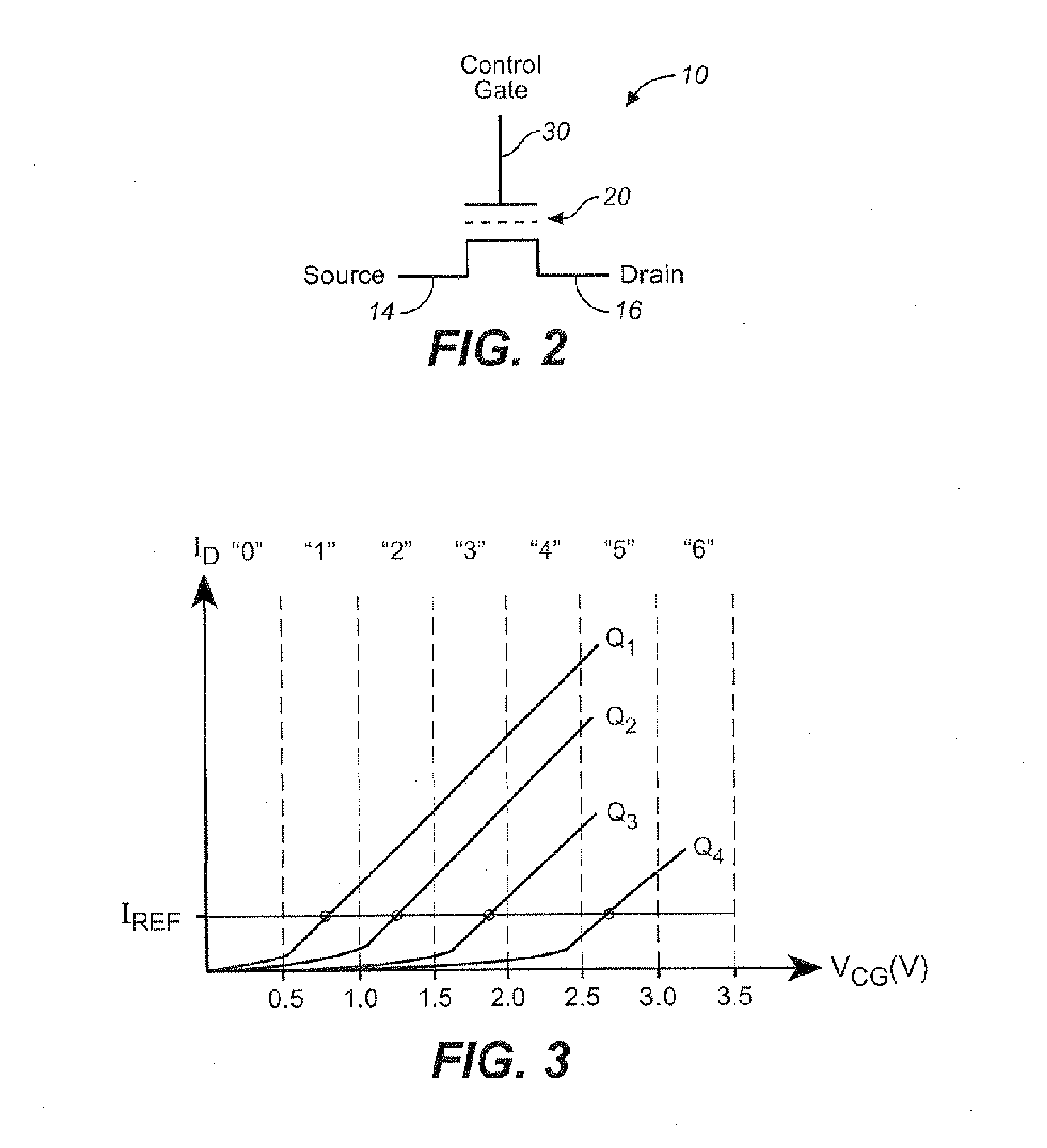
Memory System

[0035]FIG. 1 to FIG. 7 provide example memory systems in which the various aspects of the present invention may be implemented or illustrated.

[0036]FIG. 8 to FIG. 10 illustrate preferred memory and block architectures for implementing the various aspects of the present invention.

[0037]FIG. 11 and FIG. 12 illustrate the use of a satellite file system in a multi-bank system.

[0038]FIG. 1 illustrates schematically the main hardware components of a memory system suitable for implementing the present invention. The memory system 90 typically operates with a host 80 through a host interface. The memory system is typically in the form of a memory card or an embedded memory system. The memory system 90 includes a memory 200 whose operations are controlled by a controller 100. The memory 200 comprises of one or more array of non-volatile memory cells distributed over one or more integrated circuit chip. The controller 100 includes an interface 110, a processor 120, an optional co...


PUM


Abstract

A multi-bank non-volatile memory system is presented. A first of the banks has a main copy of the file system and each of the other banks has a satellite copy of the file system. The back end firmware of the controller executes a thread for each of the banks. After the boot process, during normal memory operations, each of the threads can operate using its own copy of the file system without interrupting the other threads in order to access the file system.

Description

BACKGROUND AND SUMMARY[0001]This application relates to the operation of re-programmable non-volatile memory systems such as semiconductor flash memory, and, more specifically, to the management of such system that employ a multiple bank structure.[0002]Solid-state memory capable of nonvolatile storage of charge, particularly in the form of FEPROM and flash EEPROM packaged as a small form factor card, has recently become the storage of choice in a variety of mobile and handheld devices, notably information appliances and consumer electronics products. Unlike RAM (random access memory) that is also solid-state memory, flash memory is non-volatile, and retaining its stored data even after power is turned off. Also, unlike ROM (read only memory), flash memory is rewritable similar to a disk storage device. In spite of the higher cost, flash memory is increasingly being used in mass storage applications. Conventional mass storage, based on rotating magnetic medium such as hard drives an...

Claims


Application Information

Patent Timeline
Patent Type & Authority Applications(United States)
IPC IPC(8): G06F12/16G06F12/00G06F15/177G06F12/02
CPCG06F3/061G06F3/0632G06F17/30212G06F3/0688G06F3/065G06F16/184
Inventor RAJAGOPALAN, SARANYANSCHROTER, CHARLES M.
Owner SANDISK TECH LLC
Why Eureka
Try Eureka