3D integrated circuit device having lower-cost active circuitry layers stacked before higher-cost active circuitry layer

a technology of active circuitry and integrated circuits, which is applied in the field of three-dimensional (3d) integrated circuit devices, can solve the problems of not being able to produce final substrates using general purpose substrate thinning techniques, and not being able to achieve soi circuits having structures,

Active Publication Date: 2010-12-16
GLOBALFOUNDRIES US INC
View PDF20 Cites 55 Cited by
  • Summary
  • Abstract
  • Description
  • Claims
  • Application Information

AI Technical Summary

Benefits of technology

[0009]One embodiment of the present invention provides a method for fabricating a 3D integrated circuit structure. According to the method, a first active circuitry layer wafer that includes active circuitry is provided, and a first portion of the first active circuitry layer wafer is removed such that a second portion of the first active circuitry layer wafer remains. Another wafer that includes active circuitry is provided, and the other wafer is bonded to the second portion of the first active circuitry layer wafer. The first active circuitry layer wafer is lower-cost than the other wafer.
[0010]Another embodiment of the present invention provides a 3D integrated circuit structure that includes an interface wafer including a first wiring layer, a first active circuitry layer including active circuitry, and a wafer including active circuitry. The first active circuitry layer is bonded face down to the interface wafer, and the wafer is bonded face down to the first active circuitry layer. The first active circuitry layer is lower-cost than the wafer.

Problems solved by technology

One problem experienced in the fabrication of 3D integrated circuit devices is that general purpose substrate thinning techniques do not allow the final substrate to be produced with a controlled thickness that is thin enough to allow high-density through-silicon vias with reasonable aspect ratios to be realized.
However, this technique only works for silicon-on-insulator (SOI) wafers.
Further, even with an SOI wafer, this technique does not work for SOI circuits having structures that extend below the buried oxide, such as an embedded DRAM (e-DRAM) trench.
However, this technique greatly increases the manufacturing cost.
Such protection is required because, while the SOI wafer acts as an etch stop, it does not provide selectivity between the different substrates.
However, this technique does not allow the wafers to be thinned aggressively and creates uniformity problems.
Further, for integrated circuits that require a high density of 3D vias, this technique also forces the use of high aspect ratio vias that cannot be filled with copper.
Another problem experienced in the fabrication of 3D integrated circuit devices is that stacking three or more layers to create a multi-layer stack leads to yield loss.
However, the use of such a temporary handle wafer (e.g., a glass wafer) induces overlay distortions that degrade the alignment overlay between the wafers.
That is, this technique does not allow high-precision optical alignment in subsequent lithographic steps.
However, such direct face-to-face joining is problematic because the bottom wafer (which usually is a logic wafer) must then be used as the handle wafer throughout the stacking process.
This increases the probability of catastrophic failure and loss of the entire integrated circuit, including the logic wafer that is often the most expensive wafer in the stack.

Method used


Image

  • 3D integrated circuit device having lower-cost active circuitry layers stacked before higher-cost active circuitry layer
  • 3D integrated circuit device having lower-cost active circuitry layers stacked before higher-cost active circuitry layer
  • 3D integrated circuit device having lower-cost active circuitry layers stacked before higher-cost active circuitry layer

Examples


Embodiment Construction

[0017]Preferred embodiments of the present invention will be described in detail hereinbelow with reference to the attached drawings.

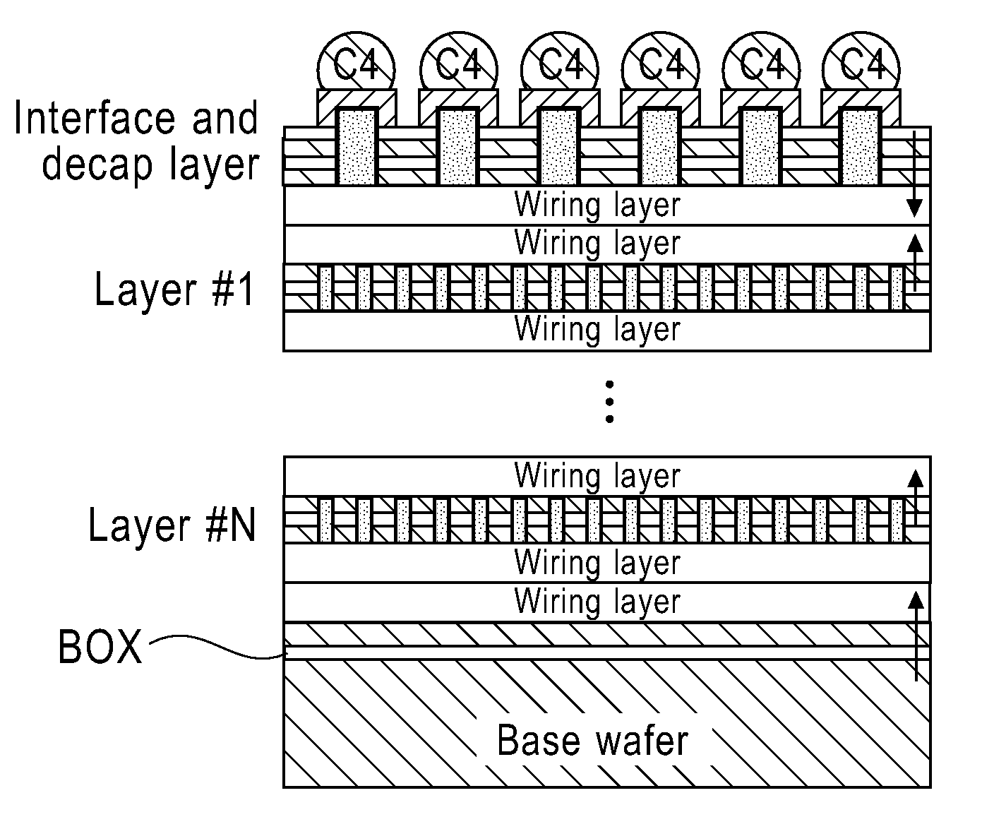
[0018]Embodiments of the present invention improve manufacturing yield by stacking lower-cost active circuitry layers of a 3D integrated circuit device before one or more higher-cost active circuitry layers. Lower-cost active circuitry layers are less expensive to manufacture than higher-cost active circuitry layers. In one exemplary embodiment, multiple memory layers of a 3D integrated circuit device are integrated with a logic layer. All of the memory layers are stacked first, and the logic layer is added to the stack last. Because the lower-cost memory layers are stacked before the higher-cost logic layer, the risk of damage to the logic layer during assembly is reduced. Thus, the present invention improves yield for 3D integrated circuit devices, and lowers manufacturing cost.

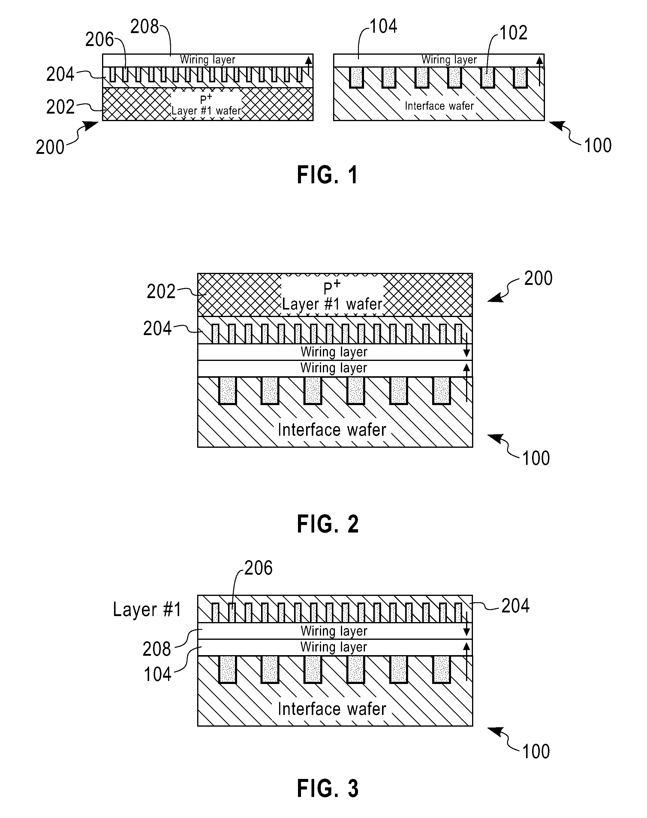
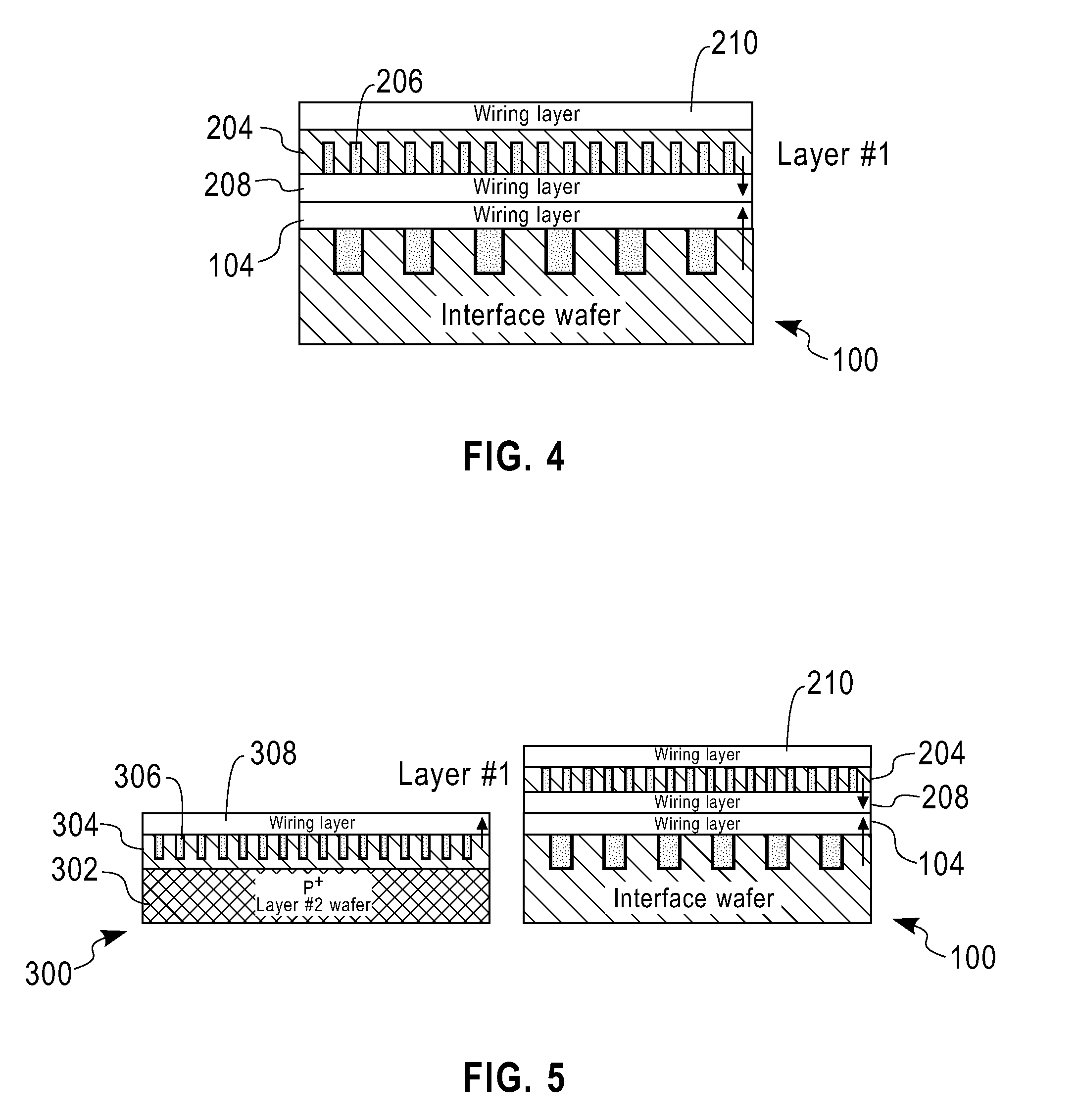
[0019]FIGS. 1 to 11 illustrate a process for fabricating a three-dimensio...


PUM


Abstract

A method is provided for fabricating a 3D integrated circuit structure. According to the method, a first active circuitry layer wafer that includes active circuitry is provided, and a first portion of the first active circuitry layer wafer is removed such that a second portion of the first active circuitry layer wafer remains. Another wafer that includes active circuitry is provided, and the other wafer is bonded to the second portion of the first active circuitry layer wafer. The first active circuitry layer wafer is lower-cost than the other wafer. Also provided are a tangible computer readable medium encoded with a program for fabricating a 3D integrated circuit structure, and a 3D integrated circuit structure.

Description

CROSS REFERENCE TO RELATED APPLICATIONS[0001]This application is related to application “3D Integrated Circuit Device Fabrication With Precisely Controllable Substrate Removal,” Ser. No. ______, now ______, and application “3D Integrated Circuit Device Fabrication Using Interface Wafer As Permanent Carrier,” Ser. No. ______, now ______, which were filed on the same day as the present application and commonly assigned therewith to International Business Machines Corporation. These related applications are incorporated herein by reference in their entirety.[0002]This invention was made with Government support under Contract No.: N66001-04-C-8032 awarded by Defense Advanced Research Projects Agency (DARPA). The Government has certain rights in this invention.FIELD OF THE INVENTION[0003]The present invention generally relates to the field of integrated circuits, and more particularly relates to the fabrication of three-dimensional (3D) integrated circuit devices.BACKGROUND OF THE INVENT...

Claims


Application Information

Patent Timeline
IPC IPC(8): H01L27/12H01L21/768
CPCH01L21/76898H01L21/8221H01L2924/00014H01L21/6835H01L2924/157H01L2924/15311H01L2924/1437H01L2924/1436H01L2924/1434H01L2924/1433H01L2924/1431H01L2924/14H01L2924/10253H01L27/0688H01L27/105H01L27/115H01L25/50H01L27/1052H01L2224/16H01L2924/00011H01L2225/06513H01L2225/06541H01L2225/06593H01L2924/37001H01L2224/92242H01L25/0657H01L25/18H01L2221/68377H01L2224/0401H01L2224/05558H01L2224/0557H01L2224/131H01L2224/16227H01L2224/2919H01L2224/32145H01L2224/32225H01L2224/33181H01L2224/73153H01L2224/73253H01L2224/83121H01L2224/83895H01L2224/94H01L2224/80001H01L2924/014H01L2224/83H01L2224/11H01L2224/73251H01L2224/08145H10B69/00H01L2224/08H10B99/00
Inventor FAROOQ, MUKTA G.HANNON, ROBERTIYER, SUBRAMANIAN S.KOESTER, STEVEN J.LIU, FEIPURUSHOTHAMAN, SAMPATHYOUNG, ALBERT M.YU, ROY R.
Owner GLOBALFOUNDRIES US INC
Why Eureka
Try Eureka