
Photoconductive materials and devices with internal photoconductive gain

a technology of photoconductive materials and optical imaging devices, applied in the direction of photometry, photometry using electric radiation detectors, instruments, etc., can solve the problems of uncertainty in the utility of meg in optical devices, digital imaging devices with poor ultraviolet spectrum detectivity, etc., and achieve high internal photoconductive gain

Inactive Publication Date: 2010-12-09
THE GOVERNINIG COUNCIL OF THE UNIV OF TORANTO
View PDF3 Cites 23 Cited by
  • Summary
  • Abstract
  • Description
  • Claims
  • Application Information

AI Technical Summary

Benefits of technology

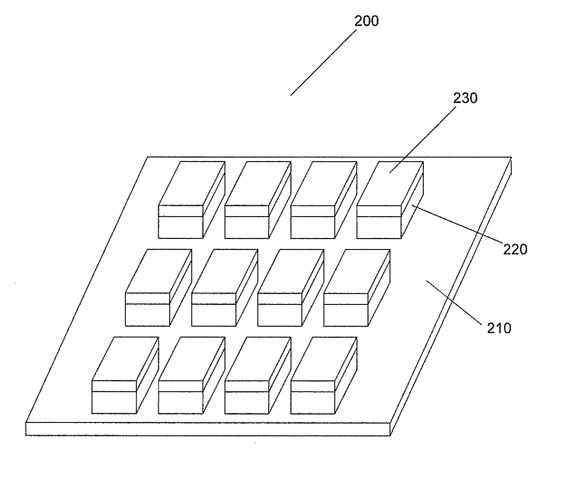
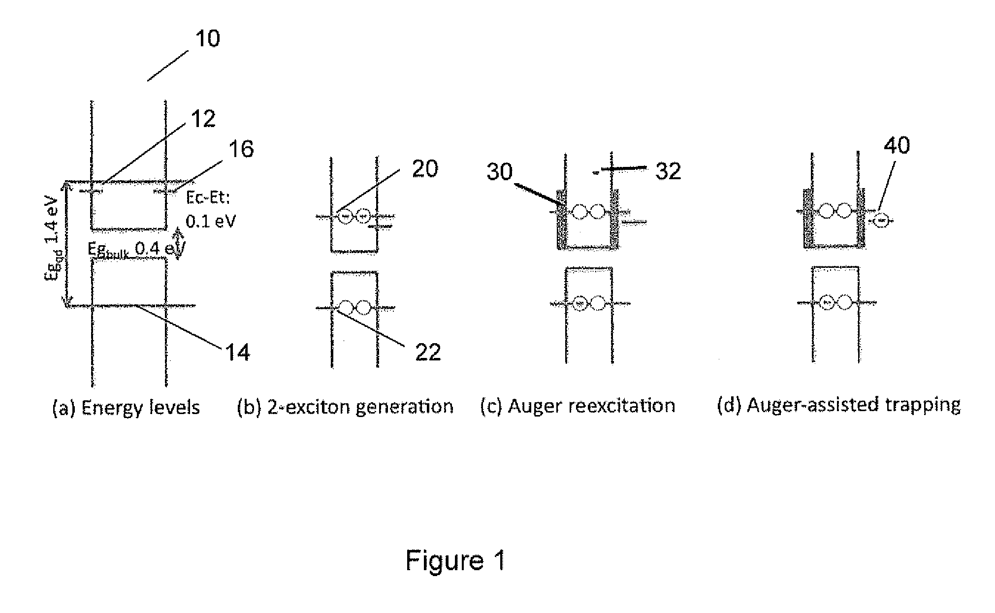
[0010]The present invention addresses this need by providing a device comprising a semiconductor or material with an electronic band gap provided in a confined geometry and capable of exhibiting multi-exciton generation (MEG) when illuminated with photons with energies above the threshold for MEG. Due to carrier-carrier Coulombic interactions, multi-excitons within the confined material efficiently recombine via Auger recombination, in which a carrier from one exciton is excited to a higher energy level relative to the band edge. Carriers excited by Auger recombination are subsequently trapped by trap states that capture carriers excited high above the band edge more efficiently than carriers near the band edge. Carriers trapped by the trap states allow for the collection and recirculation of untrapped carriers of opposite charge when used as a photoconductive device, producing high internal photoconductive gain.

Problems solved by technology

Such devices are typically limited to at most one photoelectron per photon and thereby necessitate the use of an extremely low-noise read-out scheme.
Furthermore, many digital imaging devices suffer from poor detectivity in the ultraviolet spectrum, particularly in the UV-B and UV-C spectral ranges.
As a result of these findings, the utility of MEG in optical devices, particular photovoltaic devices, is now regarded as being uncertain.

Method used


Image

  • Photoconductive materials and devices with internal photoconductive gain
  • Photoconductive materials and devices with internal photoconductive gain
  • Photoconductive materials and devices with internal photoconductive gain

Examples


example 1

Sample Preparation and Experimental Design

[0061]Nanoparticle synthesis, exchange, and processing were carried out as follows. Synthesis: PbO (0.9 g, 4.0 mmol), oleic acid (2.67 g, 9.50 mmol), and octadecene (4.73 g, 18.8 mmol) were mixed (solution A). Hexamethyldisilathiane (210 mL) was mixed with octadecene (10 mL) in a nitrogen glove box (solution B). Solution A (19.5 mL) was injected into a flask under argon and the temperature of the solution was raised to 120° C. under heavy stirring. Solution B was then injected into this flask, after which the solution was allowed to cool. When the temperature reached 35° C. the reaction was quenched with acetone (40 mL). The mixture was then washed repeatedly by suspension in toluene and precipitation in acetone.

[0062]FIG. 5 shows a TEM image of the nanoparticles used herein as well as an absorption spectrum. The materials exhibited a first excitonic absorption features at 945 nm. Three different sizes of nanoparticles were prepared by varyi...

example 2

Analysis of Results

[0068]FIG. 1(a) depicts the bands of a typical set of PbS colloidal quantum dots used herein. PbS has a bulk bandgap of 0.4 eV; the effective bandgap rises to 1.4 eV through quantum confinement in the 2 nm diameter dots investigated here. A shallow trap, resulting from PbSO3 formed by surface oxidation of PbS (26), lies just below the first confined electron state. The use of devices (27) with a single trap state lifetime facilitated interpretation of the results presented herein.

[0069]Device responsivity was determined by dividing photocurrent by the optical power incident on the device area. Internal photoconductive gain (number of registered electrons per absorbed photon) was calculated as Rhc / (qλA) where R is responsivity, h is Planck's constant, q is the electron charge, λ is the wavelength, and A is the absorption. Photocurrent dependence on illumination intensity was measured for light intensities up to 200 nW / cm2. Over this intensity range, for all wavelen...

example 3

Control Experiments to Investigate Possible Artifacts

[0074]An additional set of experiments were performed to address potential artifactual explanations of these findings. One hypothesis is that trap states could be nonuniformly distributed throughout the film, perhaps clustered closer to the air-film interface; shorter-wavelength light would then be substantially absorbed in these denser / deeper-trap regions. However, comparing internal gain spectra for devices illuminated from the top vs. the bottom, no dependence was found in the curves of FIGS. 6 and 7 on the side of optical incidence (as discussed below in reference to FIG. 9).

[0075]A second hypothesis is that, in the case of short-wavelength illumination, excited carriers could be captured directly to traps during the sub-picosecond timeframe prior to relaxation to the quantum-confined band edge without need of MEG and Auger-assisted ionization. This direct-ionization picture is incompatible with the observed universal normaliz...


PUM


Abstract

The invention provides a new class of photoconductive materials and devices, and methods for obtaining high internal photoconductive gain. The devices include a semiconductor or material with an electronic band gap provided in a confined geometry and which exhibits multi-exciton generation (MEG) when illuminated with photons with energies above the threshold for MEG. Due to carrier-carrier Coulombic interactions, multi-excitons within the confined material efficiently recombine via Auger recombination, in which a carrier from one exciton is excited to a higher energy level relative to the band edge. Carriers excited by Auger recombination are subsequently trapped by trap states that capture carriers excited high above the band edge more efficiently than carriers near the band edge. Carriers trapped by the trap states allow for the collection and recirculation of untrapped carriers of opposite charge when used as a photoconductive device, producing high internal photoconductive gain.

Description

CROSS-REFERENCE TO RELATED APPLICATION[0001]This application claims priority to U.S. Provisional Application No. 61 / 213,378 titled “PHOTOCONDUCTIVE MATERIALS AND DEVICES WITH INTERNAL PHOTOCONDUCTIVE GAIN” and filed on Jun. 3, 2009, the entire contents of which are incorporated herein by reference.FIELD OF THE INVENTION[0002]The present invention relates to photoconductive devices and optical imaging devices. More particularly, the present invention relates to confined structures for use as photoconductive detectors and photoconductive arrays with high internal photoconductive gain. The invention further relates to photoconductive imagers capable of detecting light at wavelengths well above the band gap of the material from which they are constituted. For example, the invention relates to building ultraviolet imagers using materials having a near-infrared band gap (with energy <1.8 eV); and, in another embodiment, to building visible-wavelength imagers using materials having a ba...

Claims


Application Information

Patent Timeline
IPC IPC(8): G01J1/42H01L31/08H01L27/146
CPCH01L31/035218H01L31/035209
Inventor SARGENT, EDWARD H.SUKHOVATKIN, VLAD
Owner THE GOVERNINIG COUNCIL OF THE UNIV OF TORANTO
Learn More