Organic light emitting device and preparation method thereof

a light emitting device and organic technology, applied in the field of flexible display, can solve the problems of inability to meet the requirements of display and illumination, high design requirements for phosphorescent host materials, and low light emitting efficiency of the series of materials, and achieves simple structure, strong electron withdrawal characteristic, and convenient electron injection and transport characteristics.

Active Publication Date: 2020-11-03
WUHAN CHINA STAR OPTOELECTRONICS TECH CO LTD
View PDF14 Cites 0 Cited by
  • Summary
  • Abstract
  • Description
  • Claims
  • Application Information

AI Technical Summary

Benefits of technology

[0029]Since a benzimidazolyl group shows a comparatively strong electron withdrawing characteristic, a comparatively strong modification, and has preferable electron injection and transport characteristics, it suitable for being a phosphorescent host material.
[0031](1) the benzimidazole based derivatives provided by the present invention has advantages of a simple structure and a high triplet energy level with respect to the double carbazole substituted host material, which can implement effective energy transfer of triplet exciton from a host to an object;
[0032](2) the benzimidazole based derivatives provided by the present invention has a balanced carrier mobility, which can implement effective recombination of holes and electrons in a light emitting area and increase light emitting efficiency of a device;
[0033](3) the benzimidazole based derivatives provided by the present invention has a comparatively small steric hindrance, which may notably improve glass transition temperature and heat stability and can improve the usage lifetime of a light emitting device;
[0034](4) the blue phosphorescent OLED device, which uses benzimidazole based derivatives as a light emitting layer, provided by the present invention, has excellent performance and the current efficiency, the power efficiency and the external quantum efficiency thereof all can achieve a relatively high level of performances of current blue phosphorescent devices;
[0035](5) the white phosphorescent OLED device, which uses mNBICz as a light emitting layer, provided by the present invention, has excellent performance, and the current efficiency, the power efficiency and the external quantum efficiency thereof all can achieve a relatively high level of performances of current white phosphorescent devices; and

Problems solved by technology

As a result, the design for the phosphorescent host material is highly required.
Efficiencies of red and green phosphorescent host materials and the stabilities thereof both have basically satisfied the requirements for display and illumination, however, a blue phosphorescent material is always a bottleneck for an organic electroluminescent device.
However, it should be noticed at the same time that the light emitting efficiency of the series of the materials is still comparatively low, wherein the device with a main body of mCPNBI obtains the greatest blue light emitting efficiency, but the greatest external quantum efficiency, the current efficiency and the power efficiency are still only 16.3%, 35.7 cd / A and 23.3 lm / W, which still cannot satisfy the requirements for display and illumination.

Method used


Image

  • Organic light emitting device and preparation method thereof
  • Organic light emitting device and preparation method thereof
  • Organic light emitting device and preparation method thereof

Examples


embodiment 1

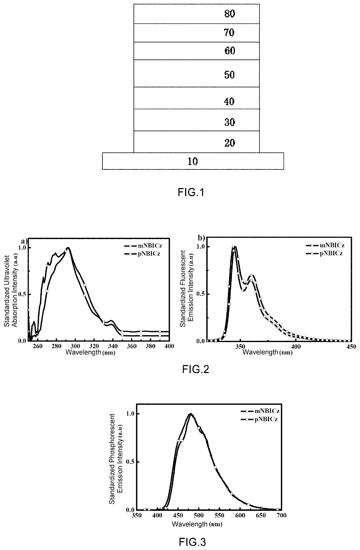
[0051]As shown in FIG. 1, the present embodiment provides an organic light emitting device which includes from the bottom to the top: an anode layer 10, a hole injection layer 20, a hole transport layer 30, an exciton blocking layer 40, an organic light emitting layer 50, an electron transport layer 60, an electron injection layer 70 and a cathode layer 80.

[0052]The material of the anode layer is a semiconductor conducting film (ITO); the material of the hole injection layer is molybdenum oxide (MoO3); the material of the hole transport layer is N,N′-diphenyl-N,N′-(1-naphthyl)-1,1′-biphenyl-4,4′-diamine (NPB) or 4,4′-cyclohexyl di[N,N-di(4-methylphenyl)phenylamine] (TAPC); the material of the exciton blocking layer is N,N′-dicarbazolyl-3,5-benzene (mCP); the material of the electron transport layer is 1,3,5-tris[(3-pyridinyl)-3-phenyl]benzene (TmPyPB); the material of the electron injection layer is LiF; and the cathode layer is Al.

[0053]Wherein, the material of the organic light em...

embodiment 2

[0085]The present embodiment further optimizes the structure of the organic light emitting device. Compared with the embodiment 1, in the organic light emitting device of the present embodiment, 4,4′-cyclohexyl di[N,N-di(4-methylphenyl)phenylamine] (TAPC) is used to replace NPB to be used as a hole transport layer, 4,4′,4″-tris(carbazole-9-yl)triphenylamine (TCTA) is used as an exciton blocking layer, and a conventional phosphorescent material mCP is used for reference. Combining with FIG. 7, it can be seen from the energy level schematic diagrams of respective compounds of the organic light emitting devices C and D that the formed structures are as follows:

[0086]the organic light emitting device C: ITO / MoO3 (10 nm) / TAPC (60 nm) / TCTA (5 nm) / Host: FIrpic (7 wt %, 20 nm) / TmPyPB (35 nm) / LiF (1 nm) / Al (100 nm), wherein the Host is mNBICz;

[0087]the organic light emitting device D: ITO / MoO3 (10 nm) / TAPC (60 nm) / TCTA (5 nm) / Host: FIrpic (7 wt %, 20 nm) / TmPyPB (35 nm) / LiF (1 nm) / Al (100 nm)...

embodiment 3

[0091]The present embodiment further prepares a structure of a white light organic light emitting device having a single host complementary color based on a good blue light device efficiency of embodiment 2. Compared with embodiment 2, in the organic light emitting device of the present embodiment, the blue light object still adopts with FIrpic, the orange light object adopts with bis(2-phenyl-benzothiazole-C2,N)(acetylacetonate)iridium (III) (Ir(bt)2 (acac)), and the stability of the white light organic light emitting device is analyzed and evaluated by adjusting a doping concentration of the orange light object. The structures of the formed four organic light emitting devices E, F, G and H are as follows:

[0092]the organic light emitting device E:

[0093]ITO / MoO3 (10 nm) / TAPC (60 nm) / TCTA (5 nm) / Host:FIrpic:Ir(bt)2(acac)

[0094](7 wt %:0.5 wt %, 20 nm) / TmPyPB (35 nm) / LiF (1 nm) / Al; wherein the Host is mNBICz;

[0095]the organic light emitting device F:

[0096]ITO / MoO3 (10 nm) / TAPC (60 nm) / ...


PUM

PropertyMeasurementUnit
mass fractionaaaaaaaaaa
internal quantum efficiencyaaaaaaaaaa

Abstract

The present invention relates to a display technical field, especially to an organic light emitting device which includes from the bottom to the top: a substrate, an anode layer, a hole injection layer, a hole transport layer, an exciton blocking layer, an organic light emitting layer, an electron transport layer, an electron injection layer and a cathode layer; the material of the organic light emitting layer includes benzimidazole derivative as illustrated in Formula 1,wherein P1, P2 and P3 are benzene rings, and at least one of R1˜R12 is a substituent having hole transport ability. The present invention further provides preparing methods for the organic light emitting layer and device.

Description

CROSS-REFERENCE TO RELATED APPLICATION[0001]This application is the U.S. national phase of PCT Application No. PCT / CN2017 / 089607 filed on Jun. 22, 2017, which claims priority to CN Patent Application No. 201710155875.2 filed on Mar. 16, 2017, the disclosures of which are incorporated in their entirety by reference herein.TECHNICAL FIELD[0002]The present invention belongs to a flexible display technical field, more particularly, to a preparation of an organic light emitting device.BACKGROUND ART[0003]In 1987, professor, Ching W. Tang, and Vanslyke adopted an ultrathin film technique which used a transparent conducting film as anode, AlQ3 as a light emitting layer, triarylated amine as a hole transport layer and Mg / Ag alloy as cathode to prepare a double-layered organic electroluminescent device (Appl. Phys. Lett., 1987, 52, 913). In 1990, Burroughes et al found an OLED in which conjugated polymer PPV is a light emitting layer (Nature. 1990, 347, 539), since then an upsurge for resear...

Claims


Application Information

Patent Timeline
Patent Type & Authority Patents(United States)
IPC IPC(8): H01L51/00C07D403/10H01L51/56C07D235/18H01L51/50H01L51/52C09K11/06
CPCC07D235/18C09K11/06H01L51/0072H01L51/56C07D403/10H01L51/5056H01L51/5004H01L51/5221H01L51/5088H01L51/5016H01L51/5072H01L51/5096H01L2251/301H01L2251/552C09K2211/1018H01L51/001H10K85/60H10K50/12H10K71/00H10K85/6572H10K50/11H10K2101/10H10K50/15H10K50/16H10K50/17H10K50/18H10K50/82H10K71/164H10K2101/30H10K2101/40H10K2102/00
Inventor PAN, BIAO
Owner WUHAN CHINA STAR OPTOELECTRONICS TECH CO LTD
Why Eureka
Try Eureka