Process for producing gray tone mask
a graytone mask and manufacturing method technology, applied in the field of graytone mask manufacturing, can solve the problems of increasing production costs, reducing the production efficiency of semi-transparent films, and not being able to adequately address or describe a method for manufacturing semi-transparent films, so as to reduce wavelength dependence
- Summary
- Abstract
- Description
- Claims
- Application Information
AI Technical Summary
Benefits of technology
Problems solved by technology
Method used
Image
Examples
example 1
Cr Oxynitride Film
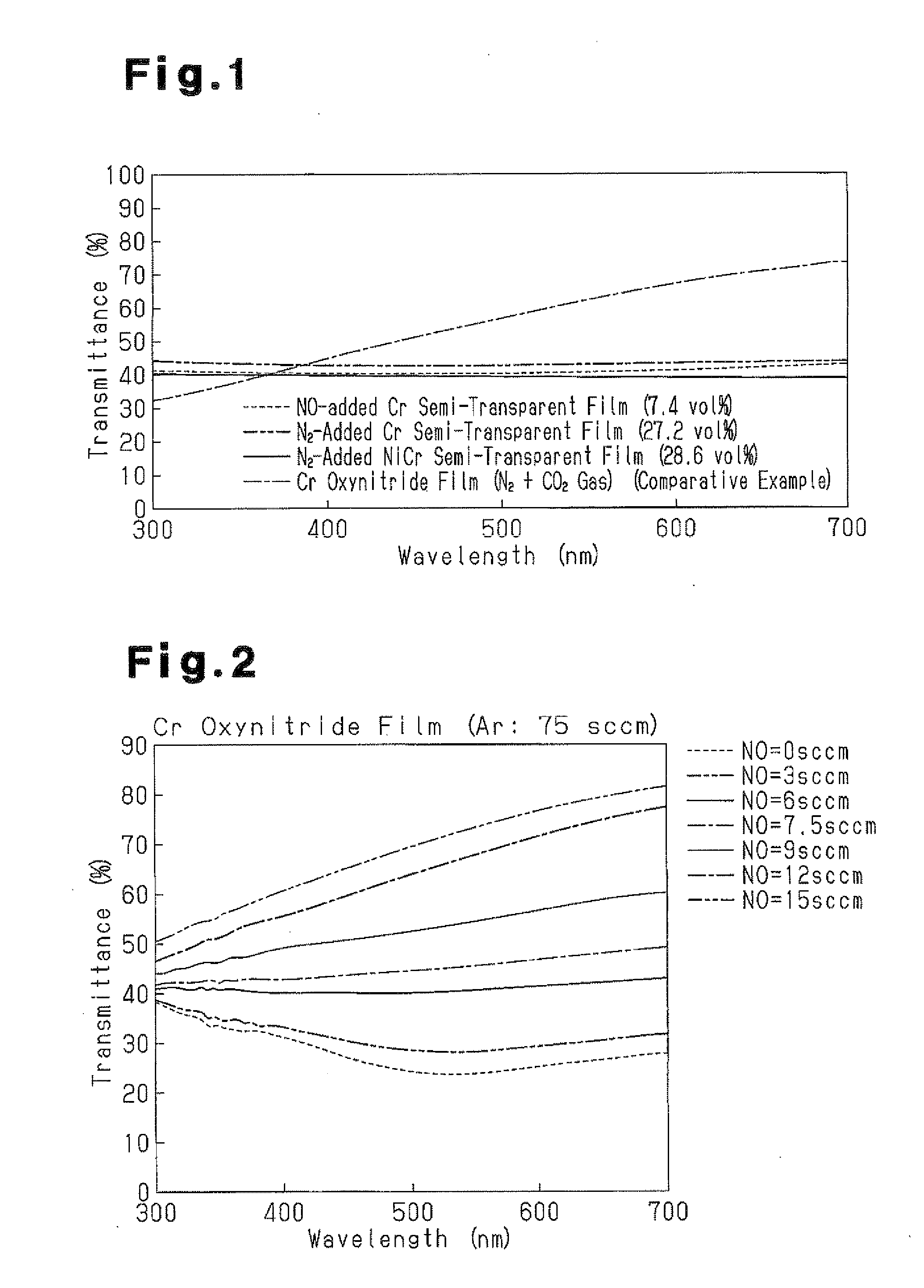
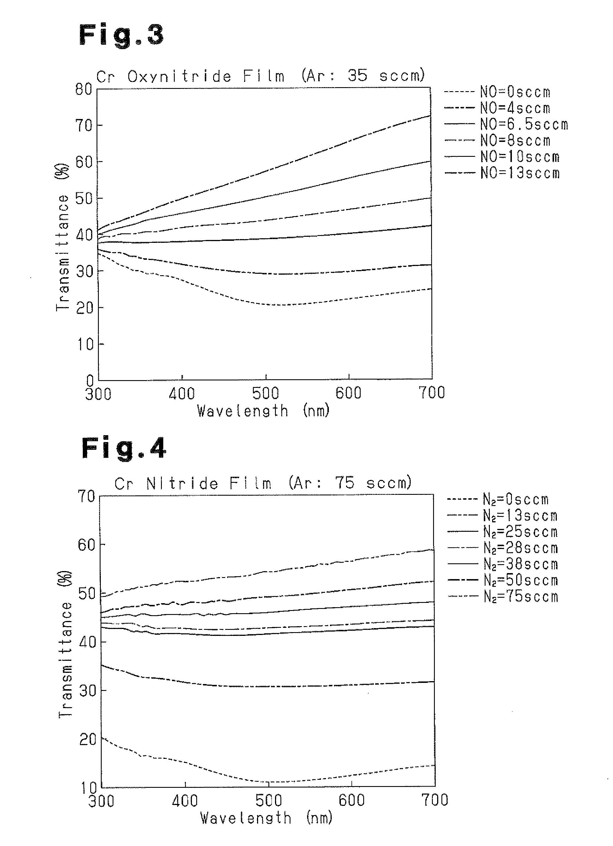
[0050]A target having a thickness of 6 mm and formed from pure Cr was used as a sputtering target, a silica substrate having a thickness of 5.0 mm was used as a substrate, and a large interback type film formation apparatus was used. Conditions that were set included the film formation temperature, which is the substrate temperature for film formation, the sputtering gas, the reactive gas, the film formation pressure, which is the pressure for film formation, and the target electric power, which is the power input to the target. The conditions were set as described below to obtain a semi-transparent film, which is a Cr oxynitride film, in example 1. In this case, the conveying speed of a substrate passing through a film formation area was controlled to maintain the film quality of the film throughout the substrate, and the film thickness of the Cr oxynitride film was adjusted to 5 nm to 20 nm, which is the film thickness when the transmittance is 30% to 50% in a se...
example 2
Cr Nitride Film
[0060]A target having a thickness of 6 mm and formed from pure Cr was used as a sputtering target, a silica substrate having a thickness of 5.0 mm was used as a substrate, and a large interback type film formation apparatus was used in the same manner as in example 1. The film formation temperature, sputtering gas, reactive gas, film formation pressure, and target electric power were set under the conditions shown below to obtain the semi-transparent film of example 2 formed by a Cr nitride film. In this case, the film thickness of the Cr nitride film, which was controlled by the conveying speed of the substrate passing through the film formation area to maintain the film quality of the film throughout the substrate, was adjusted to 5 nm to 20 nm, which is the film thickness when the transmittance is 30% to 50% in a semi-transparent film having a transmittance that is substantially not wavelength dependent.
Film formation temperature: 150° C. to 200° C.
Sputtering gas / s...
example 3
NiCr Nitride Film
[0068]A target having a thickness of 6 mm and formed from 92 atomic percent of Ni and 8 atomic percent of Cr was used as a sputtering target, a silica substrate having a thickness of 5.0 mm was used as a substrate, and a large interback type film formation apparatus was used in the same manner as in example 1. The film formation temperature, sputtering gas, reactive gas, film formation pressure, and target electric power were set under the conditions shown below to obtain the semi-transparent film of example 3 formed by a NiCr nitride film. In this case, the film thickness of the NiCr nitride film, which was controlled by the conveying speed of the substrate passing through the film formation area to maintain the film quality of the film throughout the substrate, was adjusted to 5 nm to 20 nm, which is the film thickness when the transmittance is 30% to 50% in a semi-transparent film having a transmittance that is substantially not wavelength dependent.
Film formatio...
PUM
| Property | Measurement | Unit |
|---|---|---|
| wavelength range | aaaaa | aaaaa |
| semi-transparent | aaaaa | aaaaa |
| wavelength range | aaaaa | aaaaa |
Abstract
Description
Claims
Application Information
 - R&D
- Intellectual Property
- Life Sciences
- Materials
- Tech Scout
- Unparalleled Data Quality
- Higher Quality Content
- 60% Fewer Hallucinations
Browse by: Latest US Patents, China's latest patents, Technical Efficacy Thesaurus, Application Domain, Technology Topic, Popular Technical Reports.
© 2025 PatSnap. All rights reserved.Legal|Privacy policy|Modern Slavery Act Transparency Statement|Sitemap|About US| Contact US: help@patsnap.com


