
Patterning devices using fluorinated compounds

a technology of fluorinated compounds and patterning devices, which is applied in the direction of sustainable manufacturing/processing, instruments, and final product manufacturing, etc., can solve the problems of only being used to make bottom contact circuits and devices with an order of magnitude lower performan

Active Publication Date: 2010-11-18
THE JOHN HOPKINS UNIV SCHOOL OF MEDICINE
View PDF12 Cites 83 Cited by
  • Summary
  • Abstract
  • Description
  • Claims
  • Application Information

AI Technical Summary

Benefits of technology

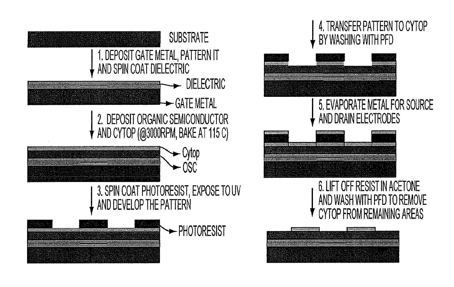
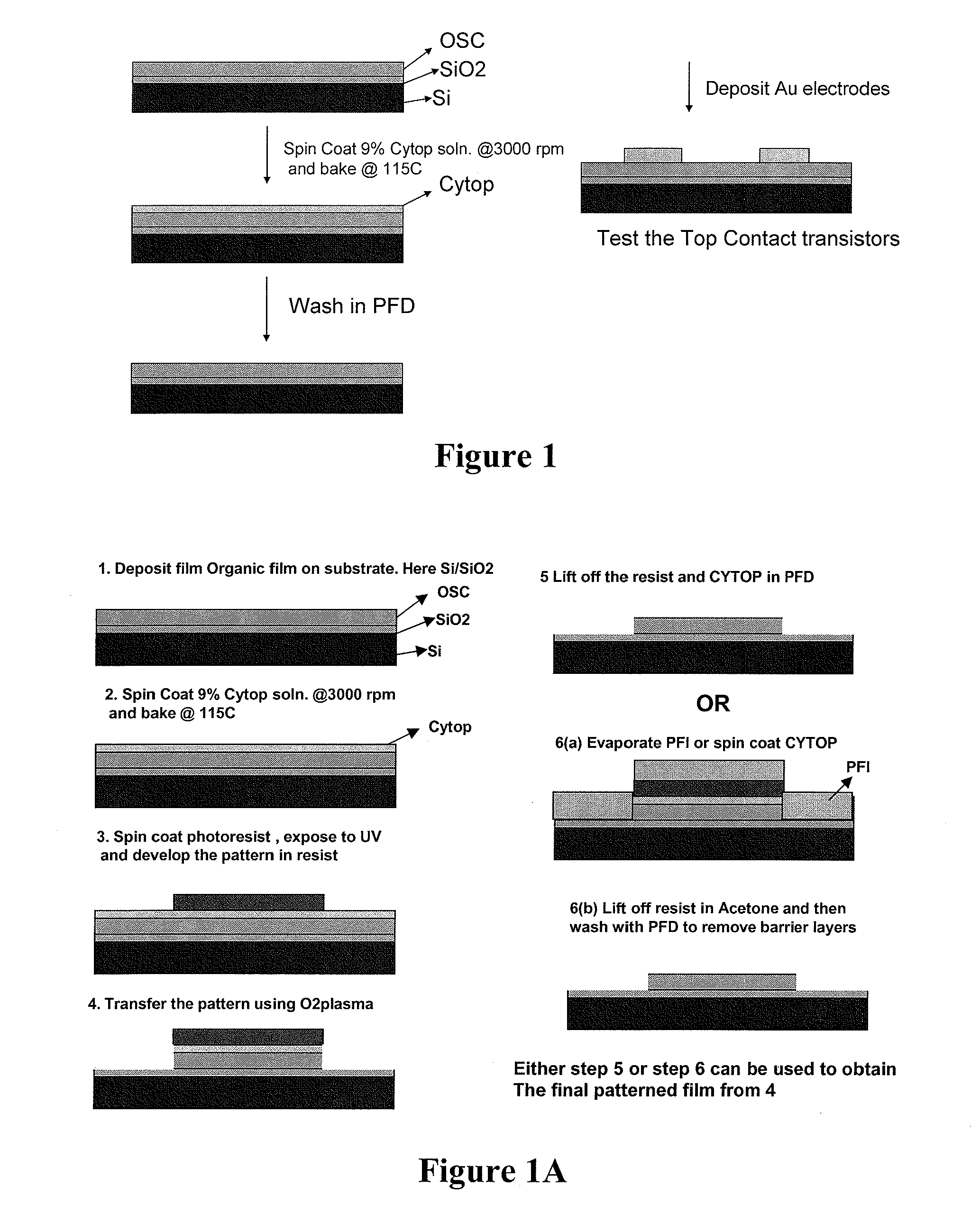
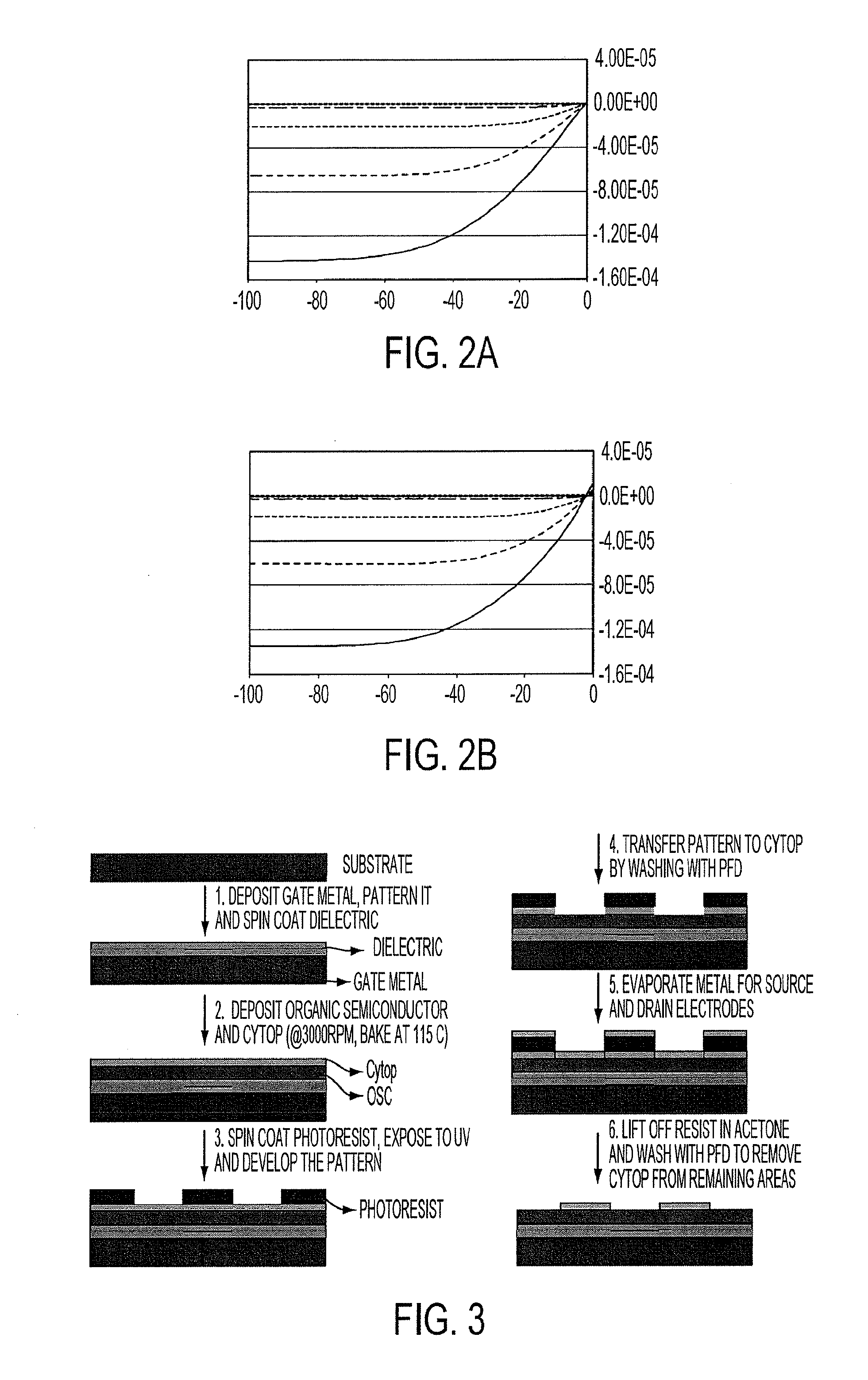
[0010]A method for producing a spatially patterned structure according to an embodiment of the current invention includes forming a layer of a material on at least a portion of a substructure of the spatially patterned structure, forming a barrier layer of a fluorinated material on the layer of material to provide an intermediate structure, and exposing the intermediate structure to at least one of a second material or radiation to cause at least one of a chemical change or a structural change to at least a portion of the intermediate structure. The barrier layer substantially protects the layer of the material from chemical and structural changes during the exposing.

Problems solved by technology

Traditional photolithographic patterning has not proven useful to pattern organic semiconductors, and organic materials in general, because of damage by the photoresist, developer and acetone during the processing (Patterning Surfaces with Functional Polymers, Zhihong Nie and Eugenia Kumacheva, Nature materials, vol.
The approach (a) can only be used to make bottom contact circuits and devices which have an order of magnitude lower performance.
The approach (b), in addition to having the problems of approach (a), also has a problem of damage to the underlying parylene layer during mechanical peel off of parylene.
The approach (c) is limited to only pentacene and has problems of lower mobility.
With the advent of solar cells and OLED devices with increasingly complex device configurations and morphologies, it has become difficult to isolate and understand the various physical processes occurring at different interfaces and in the bulk at applied bias and in the presence of light.
While devices based on organic heterojunctions have achieved significant technological milestones, the science behind them is still not completely understood and new techniques are needed to study the physics of such diodes.
Because of the “buried” nature of interfaces in vertical or bulk heterojunctions, there has been little attempt to study properties, such as conductivity, dielectric constant, and morphology, on both sides of such interfaces in one device.

Method used


Image

  • Patterning devices using fluorinated compounds
  • Patterning devices using fluorinated compounds
  • Patterning devices using fluorinated compounds

Examples


Embodiment Construction

[0028]Some embodiments of the current invention are discussed in detail below. In describing embodiments, specific terminology is employed for the sake of clarity. However, the invention is not intended to be limited to the specific terminology so selected. A person skilled in the relevant art will recognize that other equivalent components can be employed and other methods developed without departing from the broad concepts of the current invention. All references cited herein are incorporated by reference as if each had been individually incorporated.

[0029]While none of the conventional methods mentioned above are general in nature, we describe here a method of patterning materials which can be ubiquitously applied to pattern, in principle, any material and corresponding device, including devices that have spatially patterned organic semiconductor materials. However, the general concepts of the current invention are not limited to only organic semiconductor devices. Other embodime...


PUM


Abstract

A method for producing a spatially patterned structure includes forming a layer of a material on at least a portion of a substructure of the spatially patterned structure, forming a barrier layer of a fluorinated material on the layer of material to provide an intermediate structure, and exposing the intermediate structure to at least one of a second material or radiation to cause at least one of a chemical change or a structural change to at least a portion of the intermediate structure. The barrier layer substantially protects the layer of the material from chemical and structural changes during the exposing. Substructures are produced according to this method.

Description

CROSS-REFERENCE OF RELATED APPLICATION[0001]This application claims priority to U.S. Provisional Application No. 61 / 123,678filed Apr. 10, 2008, the entire content of which is hereby incorporated by reference.[0002]The U.S. Government has a paid-up license in this invention and the right in limited circumstances to require the patent owner to license others on reasonable terms as provided for by the terms of Grant No. DE-FG02-07ER46465, awarded by DOE, and of Grant No. FA9550-06-1-0076, awarded by the USAF AFOSR.BACKGROUND[0003]1. Field of Invention[0004]The current invention relates to methods of producing spatially patterned structures, and more particularly to methods of producing spatially patterned structures using fluorinated compounds. The current invention also relates to structures produced according to the methods. The current invention also relates to thin-film, lateral, organic heterojunction diodes.[0005]2. Discussion of Related Art[0006]Traditional photolithographic pat...

Claims


Application Information

Patent Timeline
IPC IPC(8): H01L51/05H01L21/04G03F7/20B32B3/10
CPCG03F7/0035H01L51/0023Y10T428/24479H01L51/102H01L51/0545Y02E10/549Y02P70/50H10K71/621H10K10/82H10K10/466H10K71/233H10K10/464H10K50/80H10K71/20H10K77/111G03F7/70058
Inventor KATZ, HOWARD EDANDHAR, BAL MUKUND
Owner THE JOHN HOPKINS UNIV SCHOOL OF MEDICINE
Learn More