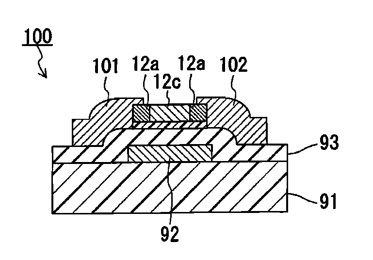
Method for producing semiconductor chip, and field effect transistor and method for manufacturing same
a manufacturing method and technology for semiconductors, applied in the direction of semiconductor devices, basic electric elements, electrical appliances, etc., can solve the problems of difficult to freely change the thickness of silicon pieces, the material to be used for substrates is limited, and the operation cannot be high-speed, etc., to achieve easy change the thickness of semiconductor pieces, reduce the cost, and the effect of flexibility in design
- Summary
- Abstract
- Description
- Claims
- Application Information
AI Technical Summary
Benefits of technology
Problems solved by technology
Method used
Image
Examples
embodiment 1
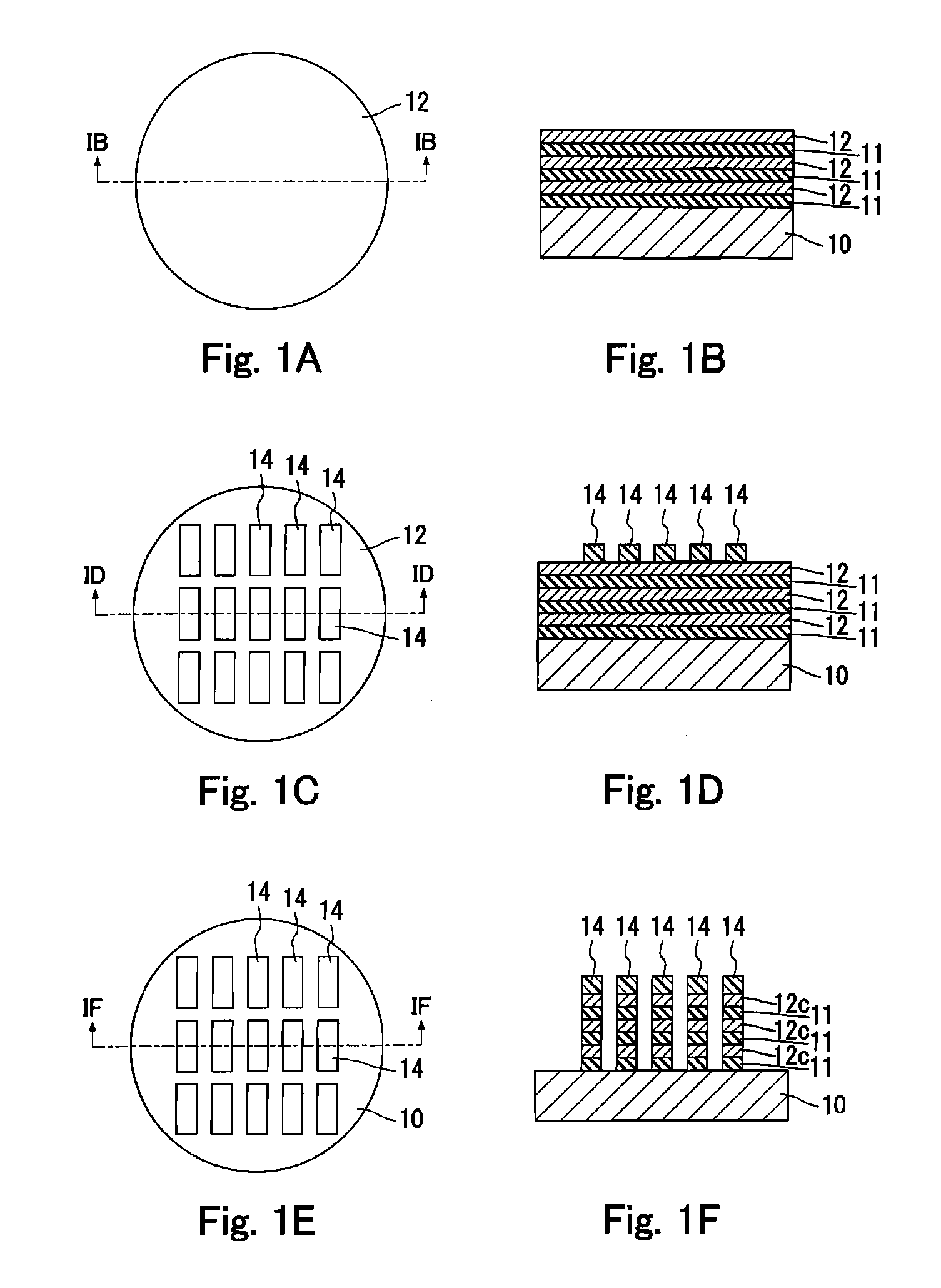
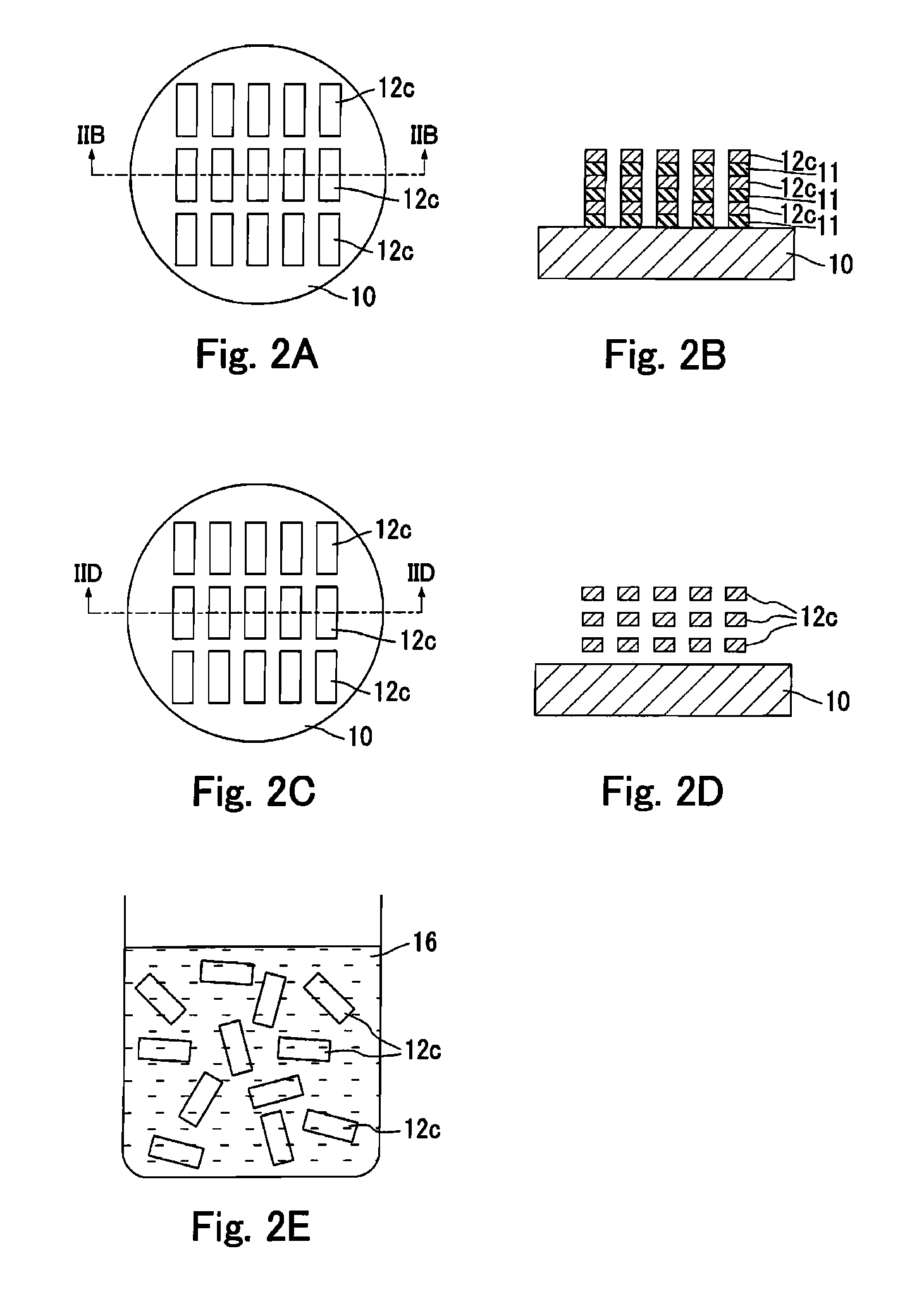
[0050]An example of the manufacturing method of the semiconductor pieces will be described below with reference to FIGS. 1A to 1F and FIGS. 2A to 2E. FIGS. 1A, 1C, 1E, 2A and 2C are top views. FIGS. 1B, 1D, 1F, 2B and 2D are the cross-sectional views of FIGS. 1A, 1C, 1E, 2A and 2C, respectively. The following diagrams are schematic views. In practice, it is possible to manufacture several hundreds or more semiconductor crystal pieces from a single wafer.
[0051]First, as shown in FIGS. 1A and 1B, three sacrificial layers 11 and three semiconductor crystal layers 12 are stacked alternately on a substrate 10. These layers are formed by a CVD method.
[0052]Examples of materials for the semiconductor crystal layer include Group IV semiconductors such as Si, Ge, SiGe and SiGeC, Group III-V semiconductors such as GaAs, GaP, GaAsP, GaSb, InP, InAs and InAsP, and Group II-VI semiconductors such as ZnS, ZnSe, CdS and CdSe. The semiconductor crystal layer 12 may be either a single crystal layer ...
embodiment 2
[0071]Embodiment 2 will describe an example of a method of manufacturing a semiconductor crystal piece having low-resistance regions at both ends thereof. FIGS. 4A to 4F show part of the manufacturing process of Embodiment 2. FIGS. 4A, 4C and 4E show top views, and FIGS. 4B, 4D and 4F show the respective cross-sectional views thereof.
[0072]First, as shown in FIGS. 4A and 4B, the sacrificial layers 11 and the semiconductor crystal layers 12 are alternately stacked on the substrate 10. Next, as shown in FIGS. 4C and 4D, a mask (resist pattern) 41 is formed on the semiconductor crystal layer 12, followed by doping with a high concentration of an impurity. This doping results in the formation of low-resistance regions 12a in part of the semiconductor crystal layers 12. The concentration of the impurity doped in the low-resistance regions 12a is, for example, around 1×1018 cm−3 to 5×1020 cm−3, (and preferably at least 5×1019 cm−3). For this purpose, multi-stage implantation in which the ...
embodiment 3
[0075]Embodiment 3 will describe an example of a method of manufacturing a semiconductor crystal piece with an insulating layer being formed on one principal surface thereof. FIGS. 6A to 6H show part of the manufacturing process of Embodiment 3. FIGS. 6A, 6C, 6E and 6G show top views, and FIGS. 6B, 6D, 6F and 6H show the respective cross-sectional views thereof.
[0076]First, as shown in FIGS. 6A and 6B, the sacrificial layer 11, the semiconductor crystal layer 12 and an insulating layer 61 are stacked on the substrate 10 in this order and the stacking is repeated. The insulating layer 61 is formed of a material having a lower etching rate than the sacrificial layer 11, as with the semiconductor crystal layer 12. Examples of a combination of the sacrificial layer 11, the semiconductor crystal layer 12 and the insulating layer 61 include a combination of the sacrificial layer 11 made of silicon oxide, the semiconductor crystal layer 12 made of polysilicon, and the insulating layer 61 m...
PUM
 Abstract
Description
Claims
Application Information
 - R&D
- Intellectual Property
- Life Sciences
- Materials
- Tech Scout
- Unparalleled Data Quality
- Higher Quality Content
- 60% Fewer Hallucinations
Browse by: Latest US Patents, China's latest patents, Technical Efficacy Thesaurus, Application Domain, Technology Topic, Popular Technical Reports.
© 2025 PatSnap. All rights reserved.Legal|Privacy policy|Modern Slavery Act Transparency Statement|Sitemap|About US| Contact US: help@patsnap.com


