
Implementing Variable Threshold Voltage Transistors

a transistor and threshold voltage technology, applied in the field of data processing, can solve the problems of complex circuit topology and limited methods

Inactive Publication Date: 2010-08-19
GLOBALFOUNDRIES INC
View PDF5 Cites 99 Cited by
  • Summary
  • Abstract
  • Description
  • Claims
  • Application Information

AI Technical Summary

Benefits of technology

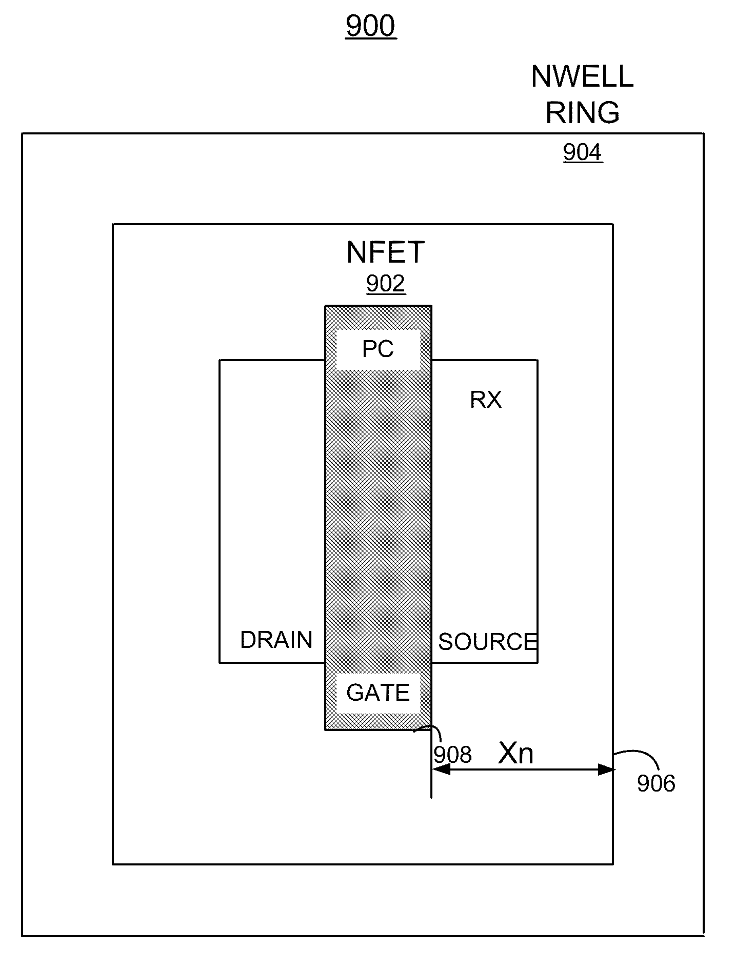
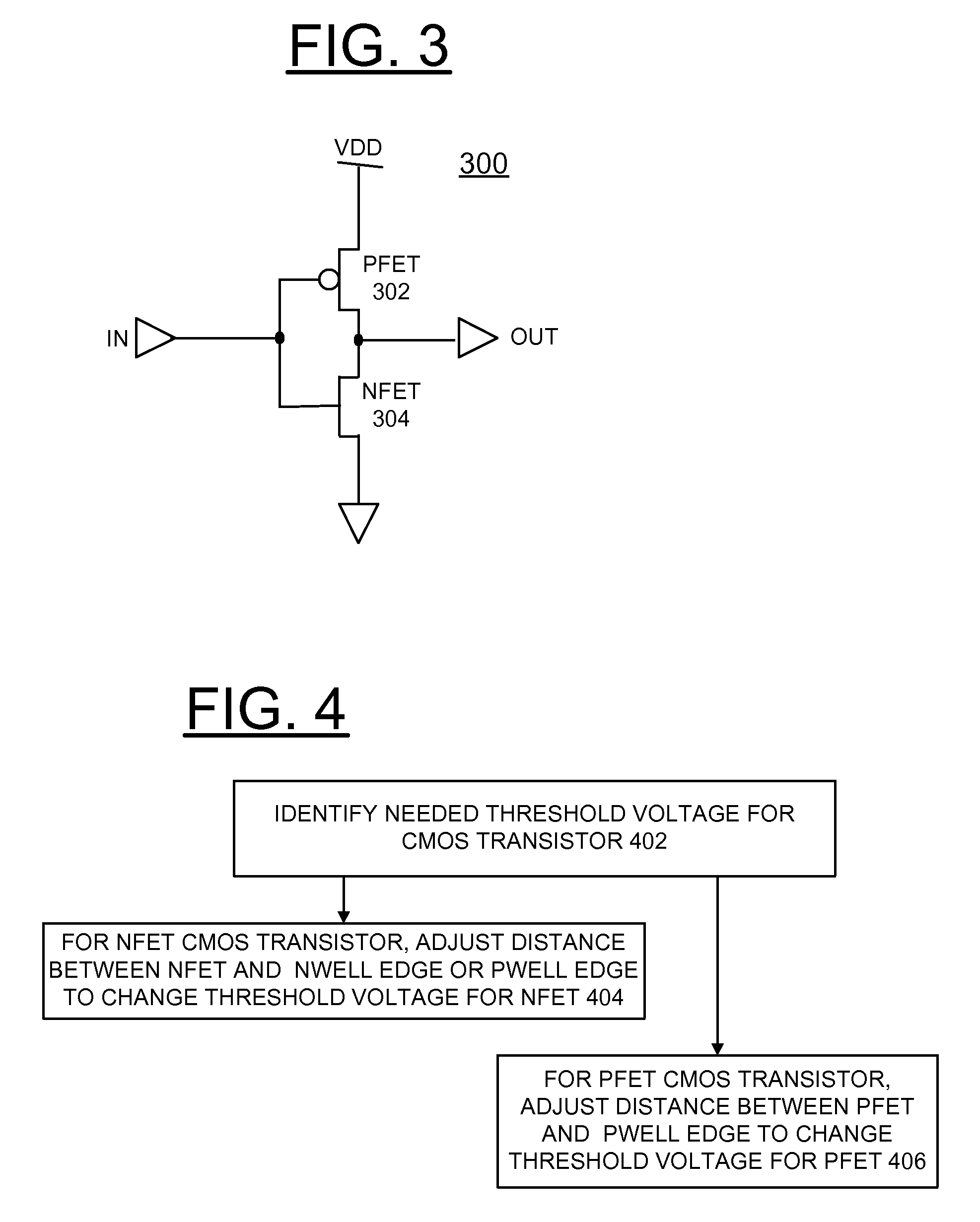
The present invention provides a circuit and method for implementing variable threshold voltage transistors in a complementary metal oxide semiconductor (CMOS) semiconductor chip, and a design structure on which the subject circuit resides. The invention utilizes the NWELL and PWELL proximity effects of the CMOS semiconductor chip to adjust the distance between an adjacent field effect transistor (FET) and an NWELL edge or PWELL edge to selectively provide a needed threshold voltage for the FET. By adjusting the distance between an NWELL edge or a PWELL edge and an adjacent NFET or PFET, the threshold voltage for the NFET transistor is changed. The invention also includes an adjacent NWELL or PWELL edge that includes an inner edge of an NWELL Ring or PWELL Ring around the entire NFET or PFET. The invention provides a solution without negative effect and overcomes many of the disadvantages of prior art arrangements.

Problems solved by technology

As a result, the circuit topology is often complex in order to overcome the fact that the CMOS technology has a fixed number of transistor types, all with fixed nominal threshold voltages.
However, this method is very limited by the number of well bias voltages available, for example, due to the physical size of using multiple biasing circuits to tune the threshold voltages of multiple transistors.
Additionally, NFETs in a P-type silicon substrate and PFETs in an N-type silicon substrate do not have wells that can be biased to an intermediate voltage between Vdd and Gnd.

Method used


Image

  • Implementing Variable Threshold Voltage Transistors
  • Implementing Variable Threshold Voltage Transistors
  • Implementing Variable Threshold Voltage Transistors

Examples


Embodiment Construction

[0021]In accordance with features of the invention, a method and circuit are provided for implementing variable threshold voltage field effect transistors using NWELL and PWELL proximity effects. The NWELL proximity effects increase the Vt of PFETs and decrease the Vt of NFETs. The PWELL proximity effects increase the Vt of NFET transistors and decrease the Vt of PFET transistors. The amount of Vt shift depends on the proximity of the FET transistor to the NWELL and PWELL edges.

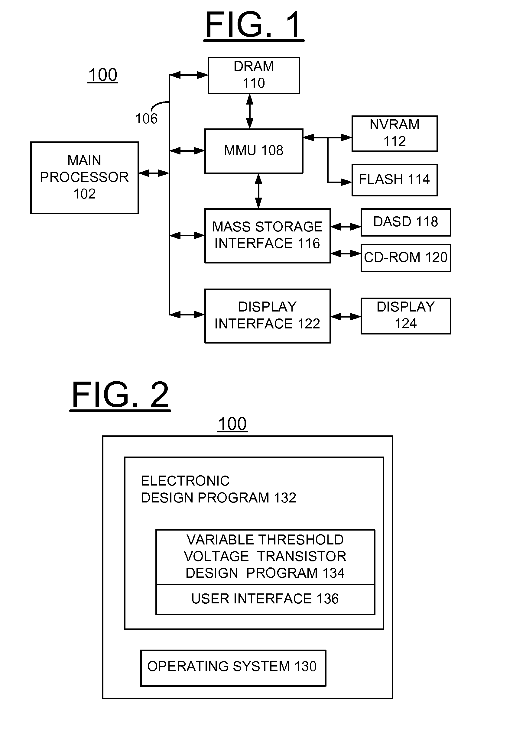
[0022]Having reference now to the drawings, in FIGS. 1 and 2 there is shown a computer system generally designated by the reference character 100 for implementing CMOS circuits having variable threshold voltage transistors in accordance with the preferred embodiment. Computer system 100 includes a main processor 102 or central processor unit (CPU) 102 coupled by a system bus 106 to a memory management unit (MMU) 108 and system memory including a dynamic random access memory (DRAM) 110, a nonvolatile random ac...


PUM


Abstract

A circuit and method for implementing variable threshold voltage transistors in a complementary metal oxide semiconductor (CMOS) semiconductor chip, and a design structure on which the subject circuit resides are provided. Variable threshold voltage transistors are provided utilizing the NWELL and PWELL proximity effects of the CMOS semiconductor chip without any additional mask steps. A distance between an adjacent field effect transistor (FET) and an NWELL edge or PWELL edge is adjusted to selectively provide a needed threshold voltage for the FET.

Description

FIELD OF THE INVENTION[0001]The present invention relates generally to the data processing field, and more particularly, relates to a circuit and method for implementing variable threshold voltage transistors, and a design structure on which the subject circuit resides.DESCRIPTION OF THE RELATED ART[0002]Complementary metal oxide semiconductor (CMOS) silicon technologies typically contain various N-channel field effect transistors (NFETs) and P-channel field effect transistors (PFETs) with fixed nominal threshold voltages (Vt).[0003]Electronic circuit designs typically use these fixed Vt transistors to realize a specified function. As a result, the circuit topology is often complex in order to overcome the fact that the CMOS technology has a fixed number of transistor types, all with fixed nominal threshold voltages.[0004]Currently, adjusting threshold voltages of CMOS transistors can be accomplished by biasing the transistor wells to a voltage other than the voltage supply rail (Vd...

Claims


Application Information

Patent Timeline
Patent Type & Authority Applications(United States)
IPC IPC(8): H01L29/78H01L21/336G06F9/45
CPCH01L27/092H01L21/823892
Inventor PASCHAL, MATTHEW JAMES
Owner GLOBALFOUNDRIES INC
Learn More