Method for planning a semiconductor manufacturing process based on users' demands

a manufacturing process and user-demand technology, applied in the field of manufacturing process planning, can solve the problems of difficulty in defining the weight of each cost function, and achieve the effect of improving the process performance of semiconductors

Inactive Publication Date: 2010-08-12
MICRON TECH INC
View PDF3 Cites 7 Cited by
  • Summary
  • Abstract
  • Description
  • Claims
  • Application Information

AI Technical Summary

Benefits of technology

[0013]The efficacy of the present invention is as follows: users can define the modulation parameters according to their recognition degrees on various process performance indexes so as to adjust the fuzzy sets of the output parameter, so the output parameter of the fuzzy system become another basis for adjusting the optimum chromosome of the genetic algorithm model, thereby not only can the optimum chromosome be the basis for improving the process performance of semiconductors, but also be suitable for users.

Problems solved by technology

However, the conventional method for planning a semiconductor manufacturing process has the following shortcomings: when users must consider a plurality of performance indexes, the fitness function of the genetic algorithm model is formed by adding a plurality of cost functions multiplied by their own weight, and each cost function respectively represents a kind of performance index and it is very difficult to define the weight of each cost function.
If the definition of the weight of any cost function is not accurate, then the result would not meet users' demands, and furthermore, each user has his different demands and it must change the weights when the users' demands are different, which is very inconvenient.

Method used


Image

  • Method for planning a semiconductor manufacturing process based on users' demands
  • Method for planning a semiconductor manufacturing process based on users' demands
  • Method for planning a semiconductor manufacturing process based on users' demands

Examples


Embodiment Construction

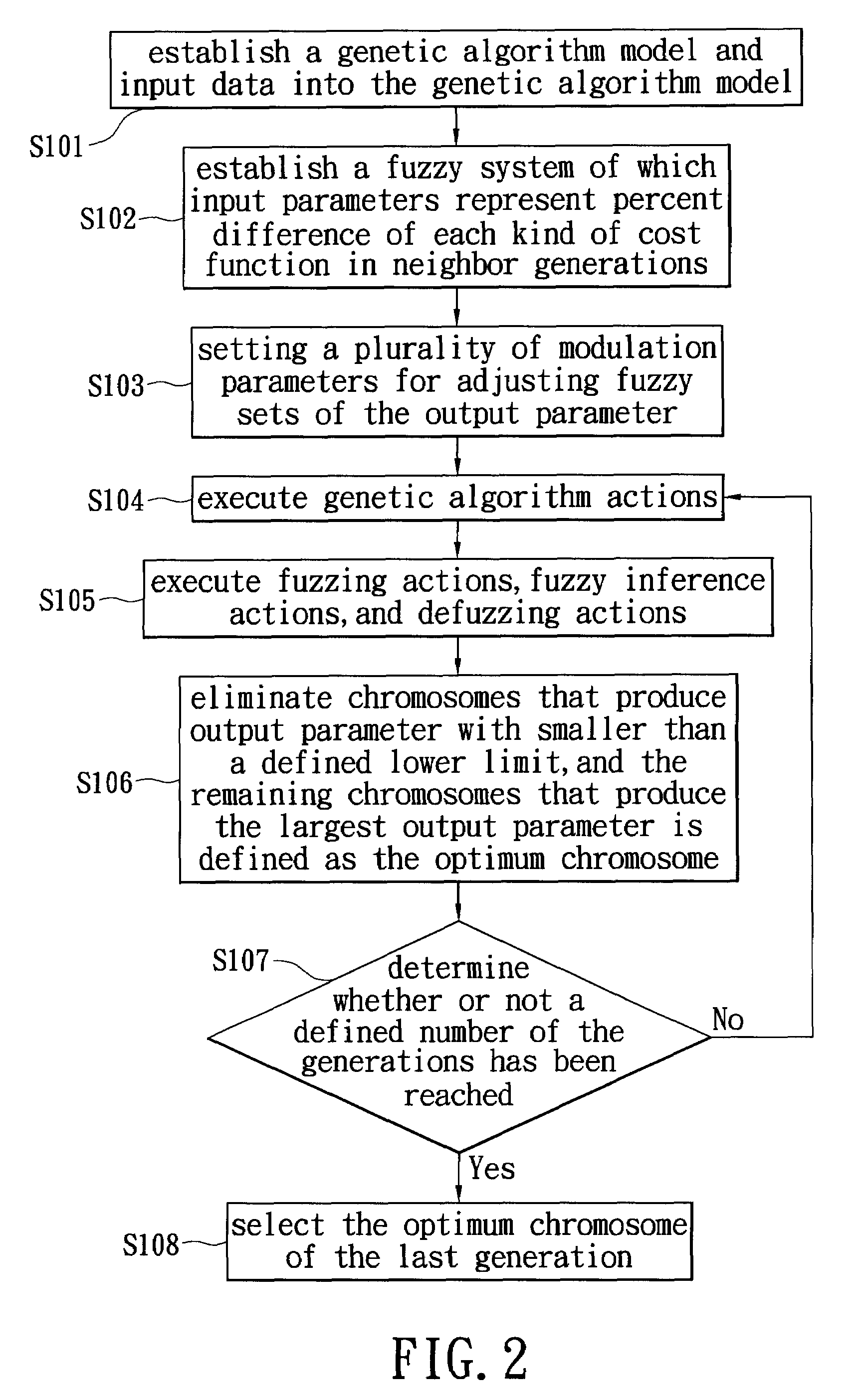
[0019]As shown in FIG. 2, the present invention provides a method for planning a semiconductor manufacturing process based on users' demands, which can be applied in a lithography process for semiconductors. The method includes steps S101-S108.

[0020]In the step S101, establish a genetic algorithm model. Predefine capable tools for each lithography layer, also predefine the process time required for each tool to manufacture each wafer of each lithography layer, and predefine setup time required for each tool to execute reticle change between each lithography layer; input data into the genetic algorithm model, wherein the data represents a group of wafer lots which need to be manufactured; and predefine the number of the wafers of each wafer lot and the type of the lithography layer of each wafer lot.

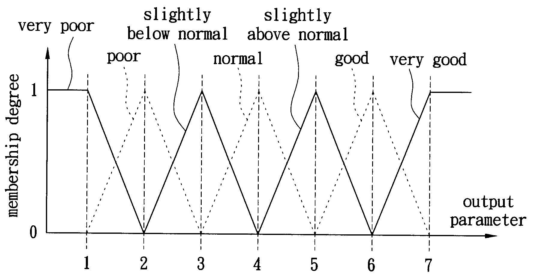
[0021]A fitness function of the genetic algorithm model is formed by adding three cost functions. The weight of each cost function is set to be the same and the number of the genetic evol...


PUM


Abstract

A method for planning a semiconductor manufacturing process based on users' demands includes the steps of: establishing a genetic algorithm model and inputting data; establishing a fuzzy system and setting one output parameter representing percent difference of each cost function in neighbor generations; setting to have a modulation parameter corresponding to each input parameter for adjusting fuzzy sets of the output parameter; executing genetic algorithm actions; executing fuzzy inference actions; eliminating chromosomes that produce output parameter smaller than a defined lower limit, and the remaining chromosomes that produces the largest output parameter is defined as the optimum chromosome, wherein the genetic algorithm actions stops being executed upon the optimum chromosome; then determining whether or not a defined number of generations has been reached, if yes, executing the optimum chromosome of the last generation; if no, continuing executing the genetic algorithm actions, thereby finding the optimum semiconductor manufacturing process for users.

Description

BACKGROUND OF THE INVENTION[0001]1. Field of the Invention[0002]The present invention relates to a method for planning a manufacturing process, and more particularly to a method for planning a semiconductor manufacturing process based on users' demands.[0003]2. Description of Related Art[0004]As shown in FIG. 1, a conventional method for planning a semiconductor manufacturing process includes the steps of:[0005]Step S10: establishing a genetic algorithm model and inputting data into the genetic algorithm model, wherein the data represents the manufacturing type of each wafers that is within a group of wafer lot that is to be manufactured;[0006]Step S20: executing genetic algorithm actions which include coding, crossover, reproduction, mutating, decoding, and so on;[0007]Step S30: determining whether or not a defined number of the generations of the genetic algorithm model has been reached, if yes, executing the step S40; if no, jumping back to the step S20; and[0008]Step S40: defini...

Claims


Application Information

Patent Timeline
Patent Type & Authority Applications(United States)
IPC IPC(8): G06N3/12G06N7/02G06F19/00
CPCG06N7/02G06N3/126
Inventor CHEN, WEI JUNCHEN, CHUN CHITIAN, YUN-ZONGLEE, YI FENGLIN, TSUNG-WEI
Owner MICRON TECH INC
Why Eureka
Try Eureka